Power architecture overview
The power solution for the 2-24 GHz front end provides regulation for the four major functional blocks in the system: the transmit chain, the receive chain, the LO chains, and the AD9081 or AD9082 MxFE with clocking solution.
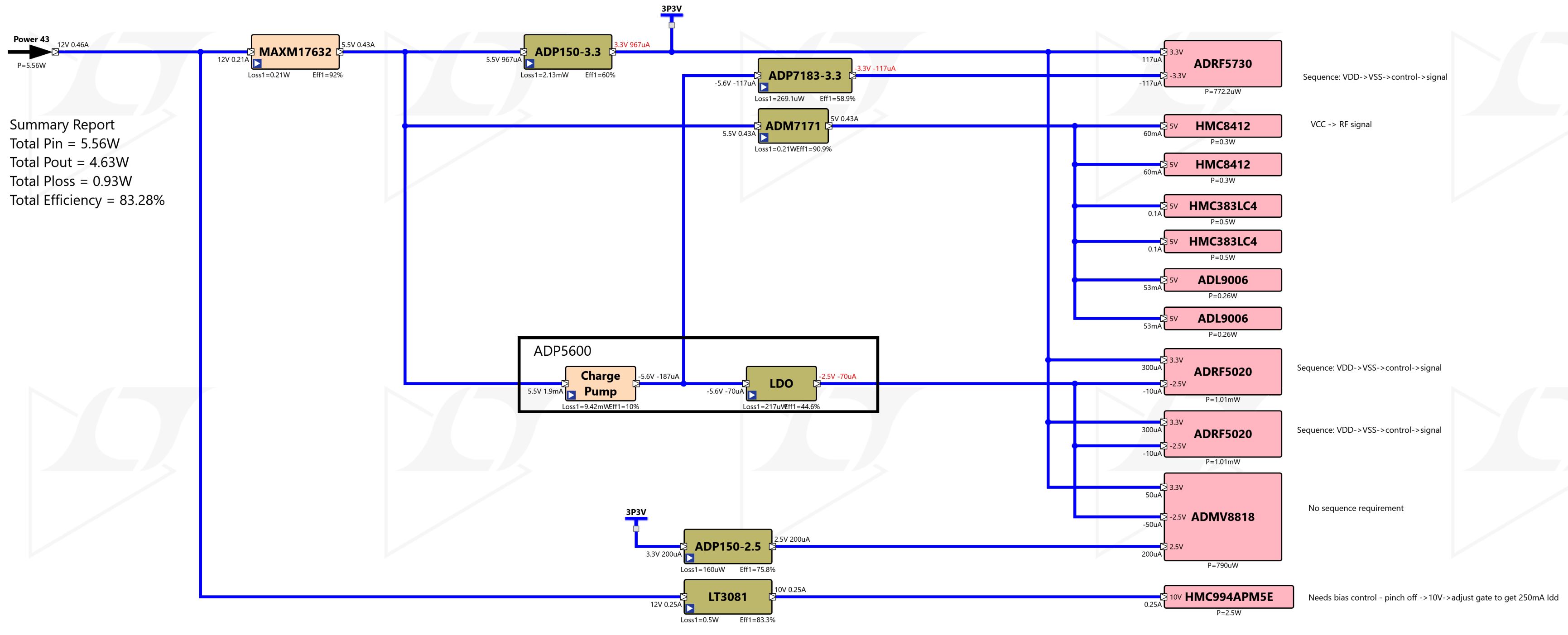
The power for the transmit chain (shown below) features two switching regulators. One is the ultra-small MAXM17632, which delivers 1 A at high efficiency from up to 36 Vin in a tiny 3 x 3 mm uSLIC™ package. The other is the ADP5600, which integrates a low ripple interleaved inverting charge pump with a high performance LDO to easily produce clean negative voltages. The sensitive signal chain power domains are regulated by low noise, high performance linear regulators.
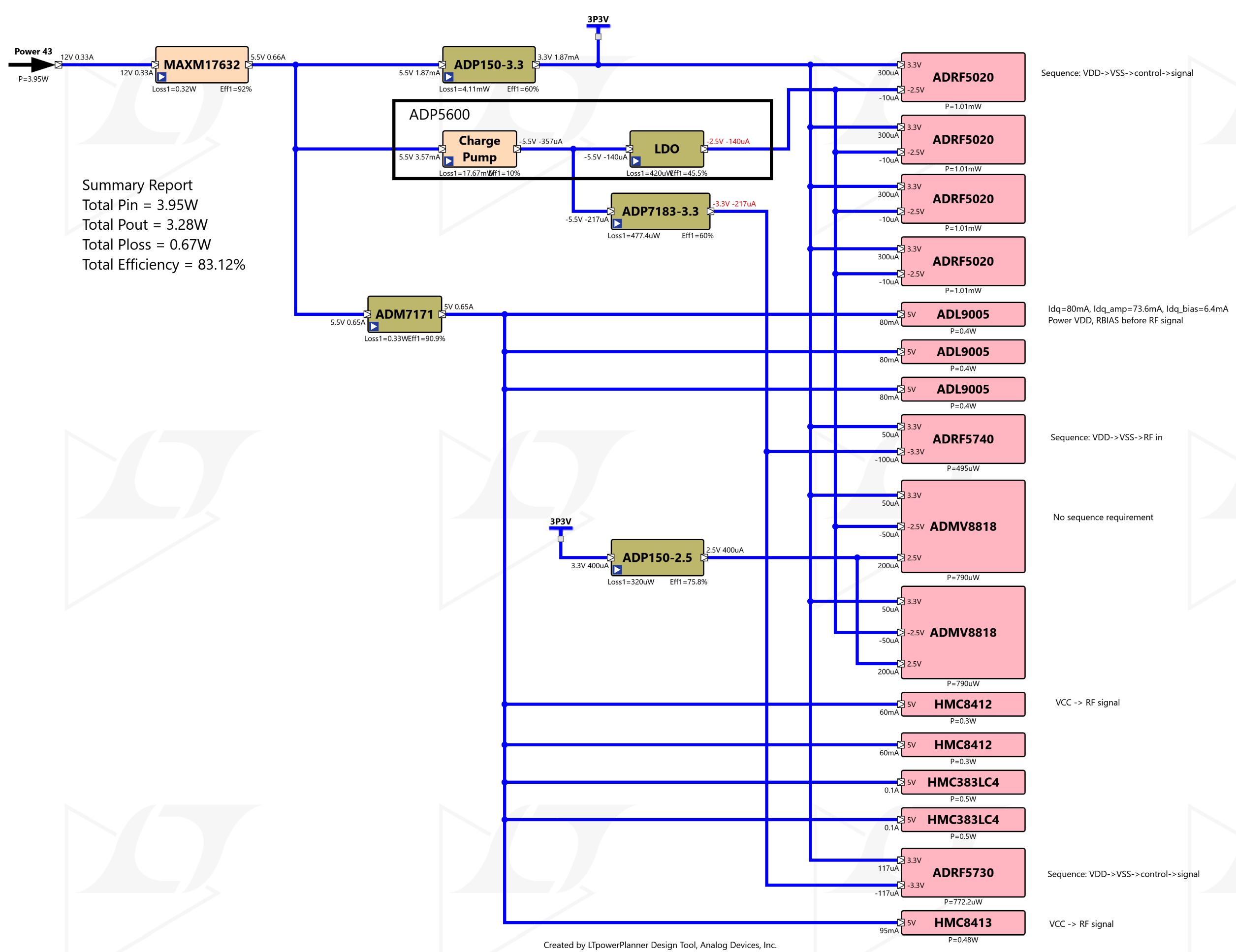
The power for the receive chain (shown below) follows a similar design philosophy as the transmit. It uses the same MAXM17632 power module and highly integrated ADP5600 to minimize the solution space. The sensitive power domains of the signal chain are regulated by low noise linear regulators.
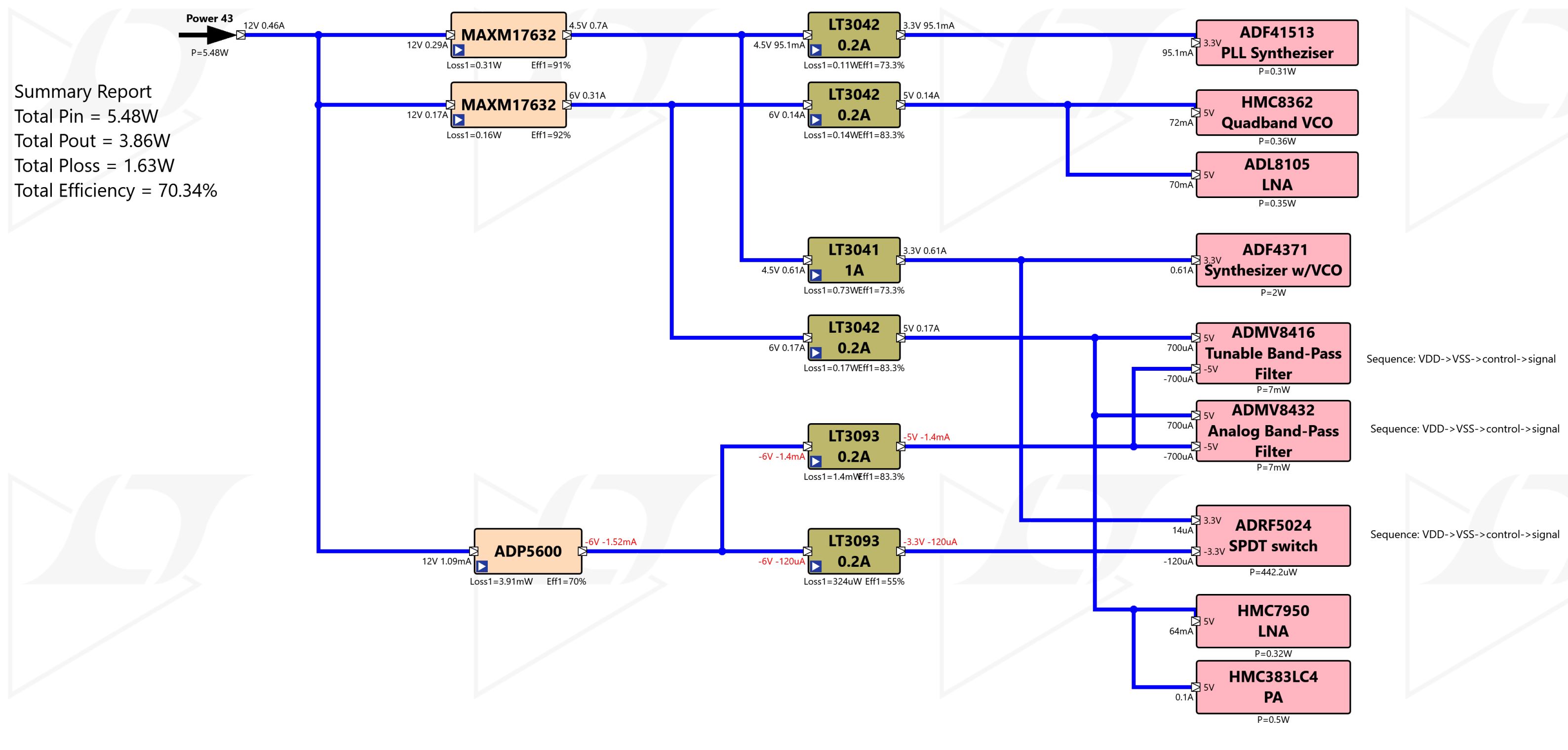
The power for the LO chains (shown below) utilizes two MAXM17632 power modules and the ADP5600. These are accompanied by low noise linear regulators for the sensitive signal chain power domains.
The power solution for the MxFE and its clock (shown below) features Silent Switcher® technology. These high efficiency regulators, LTM8051, LT8625S and LT8627S, feature low EMI and output noise. Some power domains of the MxFE chip can be driven directly from a Silent Switcher® output, while the more sensitive ICs such as the ADF4377 clock chip are further regulated by LDOs like the LT3045. The LT3045 LDO features industry leading performance with 77 dB PSRR at 1 MHz.
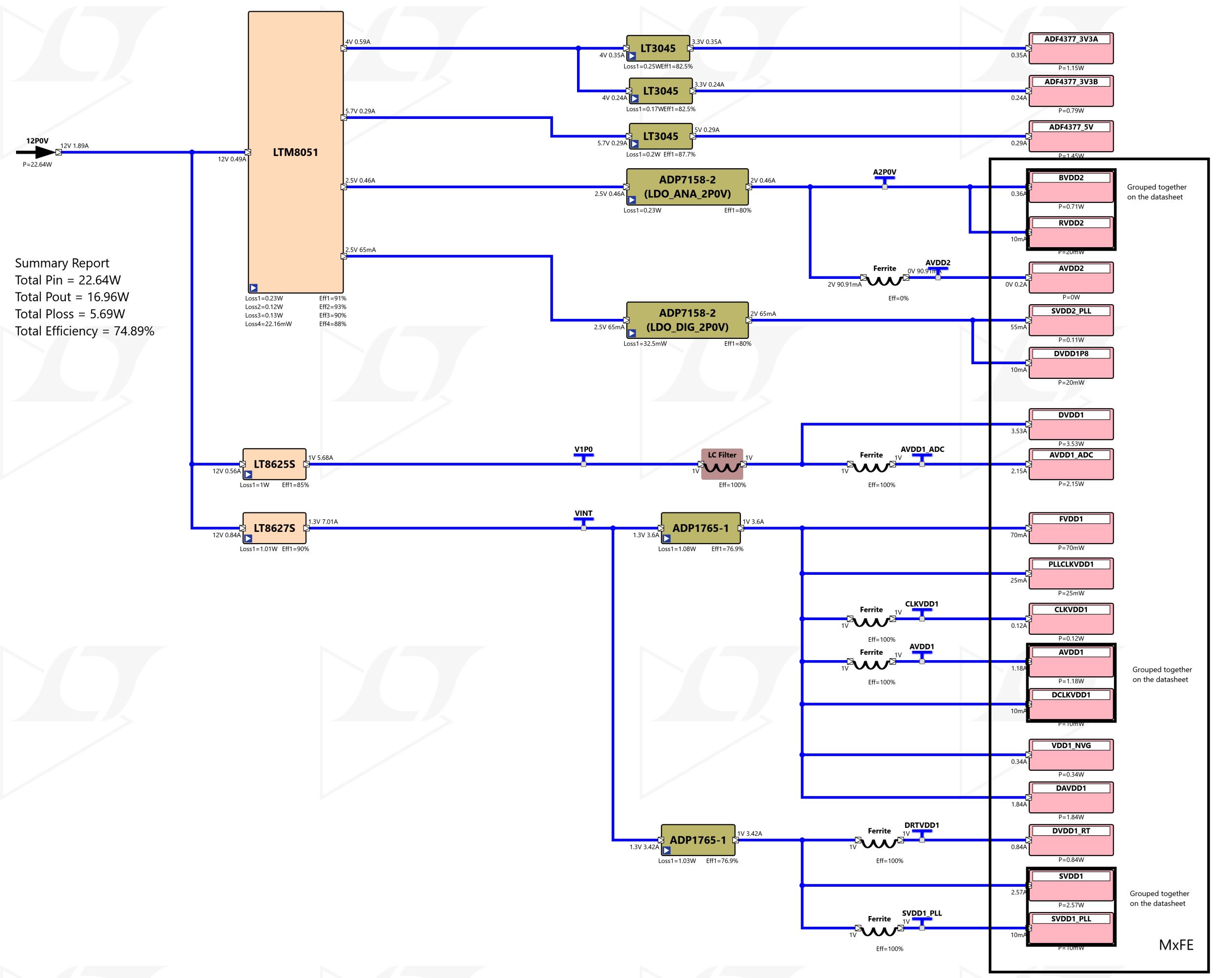
The complete LTpowerPlanner design files for the 2-24 GHz MxFE front end are available on request, see Requesting design files.