EVAL-ADICUP360 Base Board
The EVAL-ADICUP360 base board consists of two basic blocks:
A fully integrated, 3.9 kSPS, 24-bit data acquisition system that incorporates dual high performance, multichannel sigma-delta (Σ-Δ) analog-to-digital converters (ADCs), a 32-bit ARM Cortex™-M3 processor, and Flash/EE memory, realized on a single chip ADuCM360 microcontroller.
An on-board SWD interface, based on the OpenSDA platform, which is implemented with the Freescale’s К20DX128 microcontroller. This block allows using a free Software Development Toolchain to program and debug the ADuCM360 microcontroller part.
This page describes the hardware connectors, the jumpers and switches configuration options, the USB connectors, and links to download the schematics and the layout.
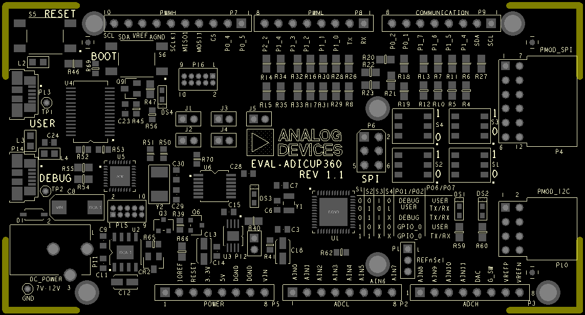
Connectors
The following connectors are populated on the base board:
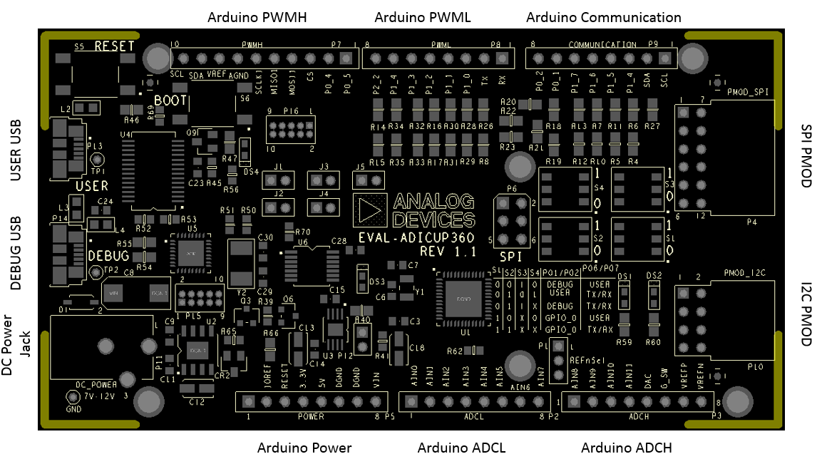
DC Power Jack: Core positive, accepts +7V to +12V DC supply voltage
DEBUG USB: Used for flash programming and debug interface
USER USB: Provides a Virtual serial port connection to ADuCM360 microcontroller
PMOD_SPI: 12-pin SPI PMOD connector
PMOD_I2C: 8-pin I2C PMOD connector
Six Arduino connectors described in the table below
Connector |
Pin No. |
Pin Name |
ADuCM360 pin or other function |
Arduino Due Pin Name |
|---|---|---|---|---|
PWMH |
10 |
SCL |
P2.0/SCL/UARTCLK |
SCL1 |
9 |
SDA |
P2.1/SDA/UARTDCD |
SDA1 |
|
8 |
AREF |
VREF+ |
AREF |
|
7 |
GND |
AGND (Analog ground) |
GND |
|
6 |
SCK |
P0.1/SCLK1/SCL/SIN |
PWM13 |
|
5 |
MISO |
P0.0/MISO1 |
PWM12 |
|
4 |
MOSI |
P0.2/MOSI1/SDA/SOUT |
PWM11 |
|
3 |
SS |
P0.3/IRQ0/CS1 |
PWM10 |
|
2 |
P0.4 |
P0.4/RTS/ECLKO |
PWM9 |
|
1 |
P0.5 |
P0.5/CTS/IRQ1 |
PWM8 |
|
PWML |
8 |
PWM5 |
P2.2/BM |
PWM7 |
7 |
PWM4 |
P1.4/PWM2/MISO0 |
PWM6 |
|
6 |
PWM3 |
P1.3/PWM1/DSR |
PWM |
|
5 |
PWM2 |
P1.2/PWM0/RI |
PWM4 |
|
4 |
PWM1 |
P1.1/IRQ4/PWMTRIP/DTR |
PWM3 |
|
3 |
PWM0 |
P1.0/IRQ3/PWMSYNC/EXTCLK |
PWM2 |
|
2 |
TX |
P0.7/POR/SOUT |
TX0 |
|
1 |
RX |
P0.6/IRQ2/SIN |
RX0 |
|
COMMUNICATION |
8 |
P0.2 |
P0.2/MOSI1/SDA/SOUT |
TX3 |
7 |
P0.1 |
P0.1/SCLK1/SCL/SIN |
RX3 |
|
6 |
P1.7 |
P1.7/IRQ7/PWM5/CS0 |
TX2 |
|
5 |
P1.6 |
P1.6/IRQ6/PWM4/MOSI0 |
RX2 |
|
4 |
P1.5 |
P1.5/IRQ4/PWM3/SCLK0 |
TX1 |
|
3 |
P1.4 |
P1.4/PWM2/MISO0 |
RX1 |
|
2 |
SDA |
P2.1/SDA/UARTDCD |
SDA |
|
1 |
SCL |
P2.0/SCL/UARTCLK |
SCL |
|
ADCH |
1 |
A8 |
AIN8/EXTREF2IN- |
A8 |
2 |
A9 |
AIN9/DACBUFF+ |
A9 |
|
3 |
A10 |
AIN10 |
A10 |
|
4 |
A11 |
AIN11/VBIAS1 |
A11 |
|
5 |
DAC |
DAC |
DAC0 |
|
6 |
G_SW |
GND_SW |
DAC1 |
|
7 |
VREF+ |
VREF+ |
CANRX |
|
8 |
VREF- |
VREF- |
CANTX |
|
ADCL |
1 |
A0 |
AIN0 |
A0 |
2 |
A1 |
AIN1 |
A1 |
|
3 |
A2 |
AIN2 |
A2 |
|
4 |
A3 |
AIN3 |
A3 |
|
5 |
A4 |
AIN4/IEXC |
A4 |
|
6 |
A5 |
AIN5/IEXC |
A5 |
|
7 |
A6 |
AIN5/IEXC |
A6 |
|
8 |
A7 |
AIN7/VBIAS0/IEXC/EXTREF2IN+ |
A7 |
|
POWER |
1 |
NC |
|
NOT USED |
2 |
IOREF |
DVdd (+3.3V) |
IOREF |
|
3 |
RESET |
RESET |
RESET |
|
4 |
3.3V |
DVdd (+3.3V) |
3V3 |
|
5 |
5V |
+5V |
5V |
|
6 |
GND |
DGND (Digital Ground) |
GND |
|
7 |
GND |
DGND (Digital Ground) |
GND |
|
8 |
Vin |
The input line of the +5V linear voltage regulator |
VIN |
|
SPI |
1 |
MISO |
P0.0 |
MISO |
2 |
+5 |
+5 |
+5 |
|
3 |
SCLK |
P0.1 |
SCLK |
|
4 |
MOSI |
P0.2 |
MOSI |
|
5 |
RESET |
RESET |
RESET |
|
6 |
GND |
DGND |
GND |
|
SPI_PMOD |
1 |
CS |
P1.7 |
CHIP SELECT |
2 |
MOSI |
P1.6 |
MOSI |
|
3 |
MISO |
P1.4 |
MISO |
|
4 |
SCLK |
P1.5 |
SCLK |
|
5 |
GND |
DGND |
GND |
|
6 |
VDD |
DVDD |
VDD |
|
7 |
INT |
P1.0 |
INT |
|
8 |
RESET |
P1.1 |
RESET |
|
9 |
GPIO |
P1.2 |
GPIO |
|
10 |
GPIO |
P2.2 |
GPIO |
|
11 |
GND |
DGND |
GND |
|
12 |
VDD |
DVDD |
VDD |
|
I2C_PMOD |
1 |
SCL |
P2.0 |
SCL |
2 |
SCL |
P2.0 |
SCL |
|
3 |
SDA |
P2.1 |
SDA |
|
4 |
SDA |
P2.1 |
SDA |
|
5 |
GND |
DGND |
GND |
|
6 |
GND |
DGND |
GND |
|
7 |
VDD |
DVDD |
VDD |
|
8 |
VDD |
DVDD |
VDD |
Jumper Configuration
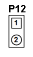
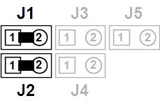
There are 3 jumpers groups on the EVAL-ADICUP360 base board:
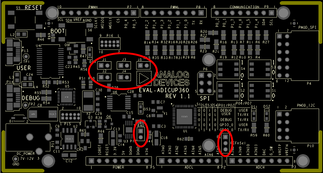
Jumper P12
Configuration |
Function |
|---|---|
|
ADuCM360 is powered from the linear voltage regulator on the baseboard |
|
ADuCM360 is not powered from the baseboard and may be powered from the application shield |
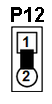
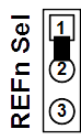
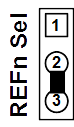
Jumper REFnSel
Configuration |
Function |
|---|---|
|
ADuCM360 VREF- pin connected to Analog GND |
|
ADuCM360 VREF- pin connected to the ADCH connector, pin 8 |
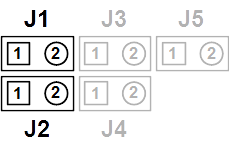
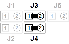
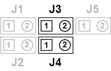
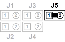
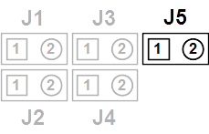
Jumpers J1, J2, J3, J4, J5
Configuration |
Function |
|---|---|
|
ADuCM360’s UART pins are connected to the Virtual serial port of the Debug adapter |
|
ADuCM360’s UART pins are not connected to the Virtual serial port of the Debug adapter |
|
ADuCM360’s SWD lines are connected to the Debug adapter. ADuCM360 can be programmed |
|
ADuCM360’s SWD lines are not connected to the Debug adapter. ADuCM360 cannot be programmed |
|
ADuCM360’s RESET line is connected to the Debug adapter. The button B1 can be used to invoke the Debug adapter’s Bootloader. |
|
ADuCM360’s RESET line is not connected to the Debug adapter. The button B1 is just an ADuCM360 reset button. |
USB/Connector Multiplexer
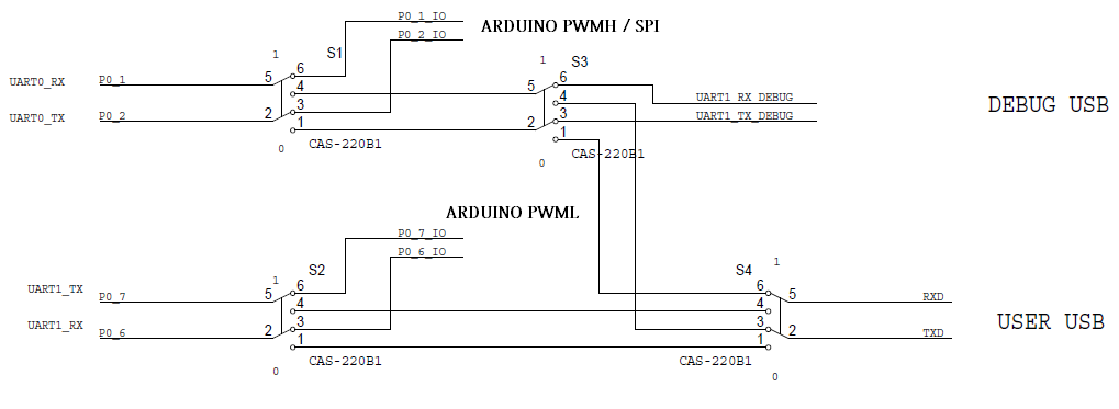
There are 4 switches on the EVAL-ADICUP360 base board, which are used to multiplex pairs of pins (P0.1/P0.2, and P0.6/P0.7) to various different connectors on the board. Depending on how the pins are configured you may route them to the USB ports, use them for SPI communication or for UART communication.
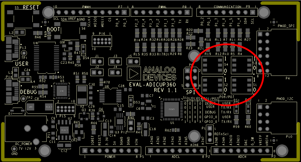
Switches S1, S2, S3, S4
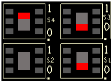
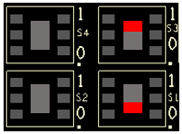
The S1, S2, S3, S4 switches are used to route the P0.1/SCLK1/SCL/SIN, P0.2/MOSI1/SDA/SOUT, P0.6/IRQ2/SIN and P0.7/POR/SOUT pins when they have been assigned a UART function to either the Arduino I/O and the PMOD connectors or to the Virtual Serial ports implemented via the USER USB or the DEBUG USB connectors. Each pin can be routed separately, but the routing is usually done for the pairs TxD/RxD.
Most commonly used configurations are given in the table below. For any other more ‘exotic’ configuration, consult with the Schematics and the Layout of the board.
ADuCM360’s pair of pins |
Required connection |
Configuration |
|---|---|---|
P0.1/SCLK1/SCL/SIN P0.2/MOSI1/SDA/SOUT |
to the User USB (FT232RL) |
|
to the Debug USB (mbed’s Serial Port) |
|
|
to the Arduino PWMH (pin 6, pin 3) and the SPI header (pin 1, pin 3) |
|
|
P0.6/IRQ2/SIN P0.7/POR/SOUT |
to the User USB (FT232RL) |
|
to the Arduino PWML (pin 1, pin 2) |
|
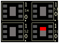
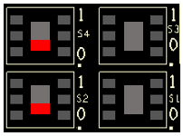
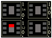
Switch Schematic
Here is the schematic of the switching network, the switches allow to route the P0.1/P0.2 and P0.6/P0.7 signals to multiple connector depending how you want to configure the pins. Above are the common configurations, but for complete details please reference the diagram.
Buttons
The EVAL-ADICUP360 base board provides two buttons RESET and BOOT.
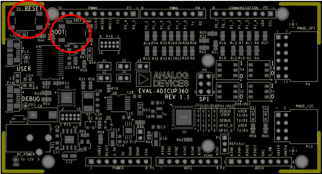
Button |
Function |
|---|---|
RESET |
Provides a hardware RESET to ADuCM360 microcontroller. If the RESET line is connected to the Debug adapter, this button can be used to invoke the Debug adapter’s Bootloader, see section Jumper Configuration. |
BOOT |
When BOOT is held down during the reset and after, the ADuCM360 microcontroller enters UART download mode via P0.1 and P0.2. In this case, the user can download program via DEBUG USB or USER USB, depending on the jumpers settings, see section Jumper Configuration. BOOT button should be held press while a reset from the button is performed. |
Schematics, PCB Layout, Bill of Materials
Download
EVAL-ADICUP360 Design & Integration Files
Schematic
PCB Layout
Bill of Materials
Allegro Project