EVAL-CN0418-ARDZ Shield Overview
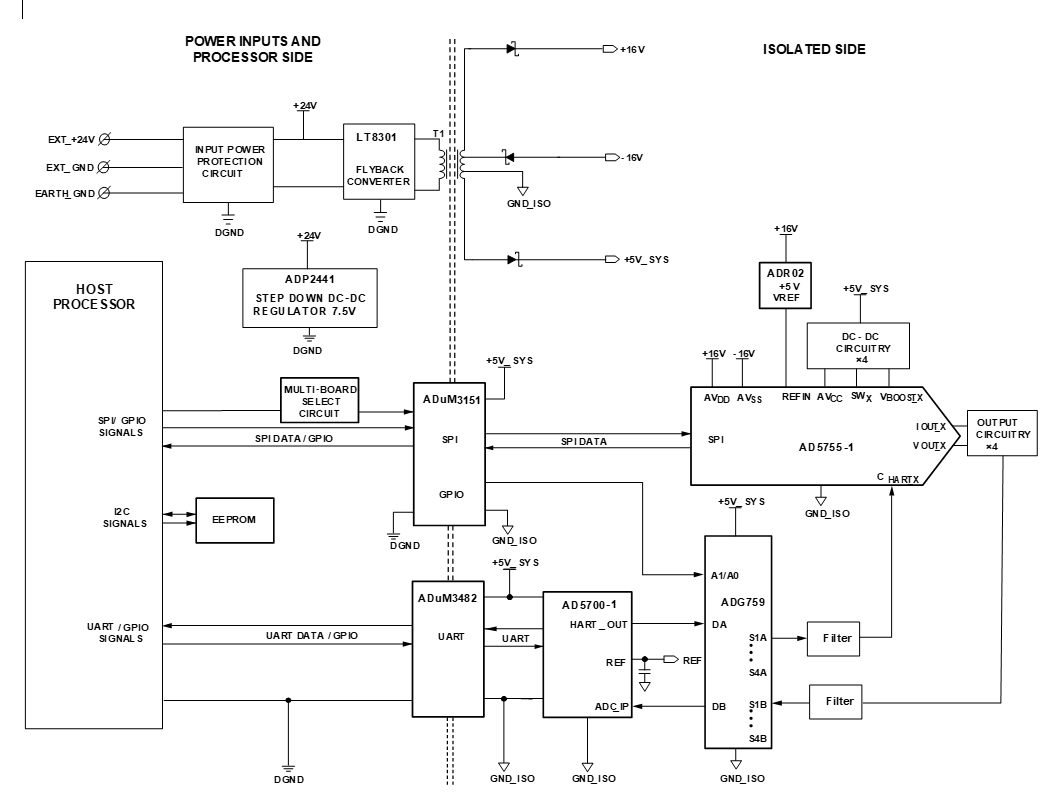
The circuit shown in Figure 1 provides a complete, fully isolated and highly flexible, 4-channel analog output system suitable for programmable logic controllers (PLCs) and distributed control system (DCS) applications that require ±5 V, ±10 V voltage and 4 mA to 20 mA current output with HART-compatibility. All outputs are protected from transients and are suitable for the most harsh industrial environments.
The HART compatibility of this module provides a complete field communications solution that is simple to use, low cost, and extremely reliable.
The circuit is powered from a standard 24 V bus supply, with on-board filtering and protection circuitry. Because many factories and industrial environments power their PLC/DCS from a 24 V standard bus line, this module is easy to integrate into any existing system. This module can also be powered from other standard supplies, starting from 12 VDC to 28 VDC
This user guide will discuss how to use the EVAL-EVAL-ADICUP3029 and evaluation software to configure and collect data from the EVAL-CN0418-ARDZ Evaluation Board (CN-0418 Board).
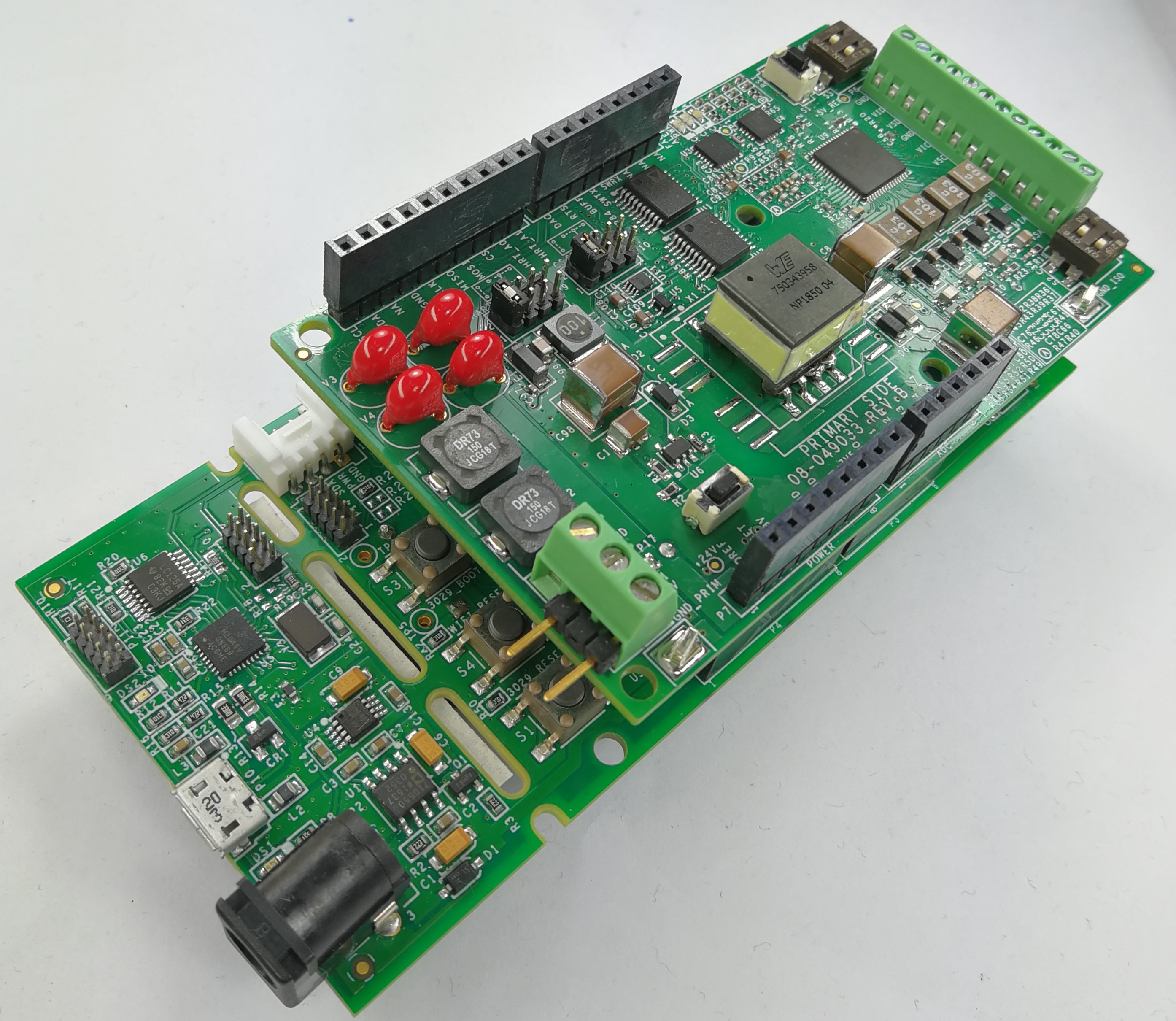
EVAL-CN0418-ARDZ attached to EVAL-ADICUP3029
Simplified functional block diagram
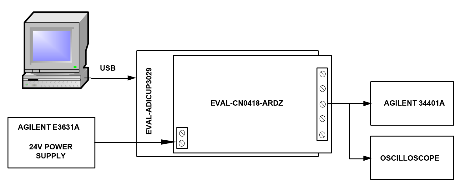
General Setup
Equipment
PC with a USB port and Windows 7 (32-bit) or higher
Serial Terminal Software (Putty/TeraTerm or similar)
DC Power Supply (+12 V to +24 V / 1 A) or equivalent bench supply (optional)
Precision voltage and current source (for output measurement)
USB type A to micro USB type A cable
CN0418 Evaluation Software
The EVAL-CN0418-ARDZ (CN-0418 Board) connects to the EVAL-ADICUP3029 (ADICUP3029 Board)
The EVAL-ADICUP3029 (ADICUP3029 Board) connects to the PC via the USB cable.
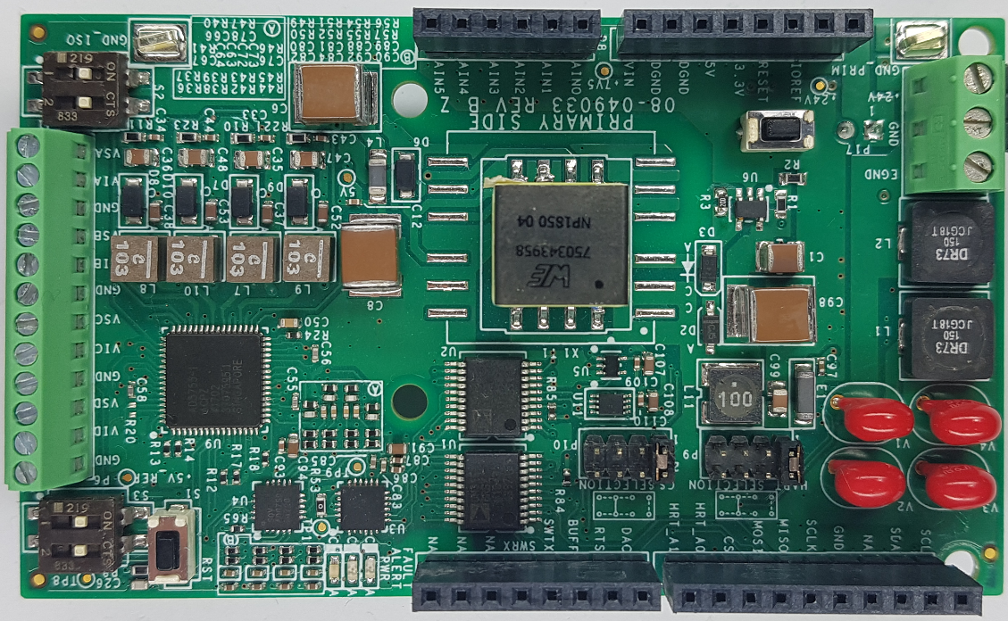
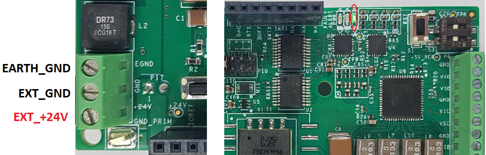
Terminal block P1 is the power supply input (input:+24V DC)
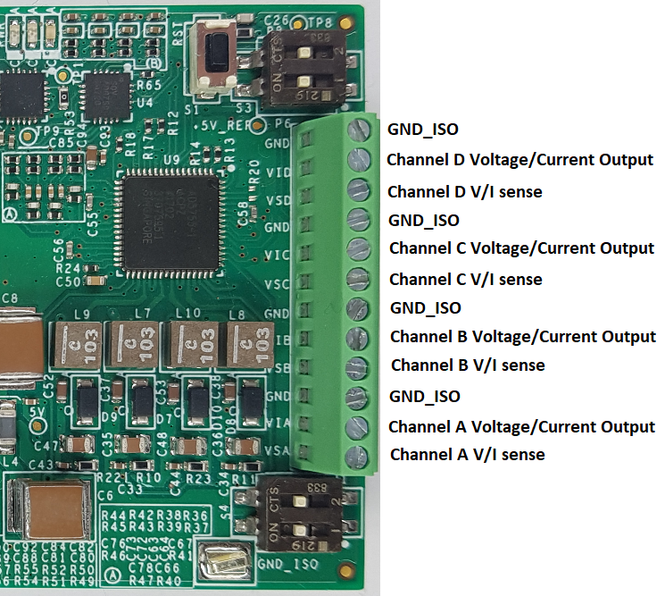
Terminal blocks P6 provide the quad channel voltage output (-10V to +10V), and Current output (0mA to 24mA) and standard 4 mA to 20 mA HART compatible current inputs.
Power Supply Considerations and Configuration (P1)
Terminal block P17 is the power supply input (input range:+12V to +36V DC). The EARTH terminal can be connected to an external earth connection, to the GND terminal or left floating if an external earth connection is not used. The Green power LED should lit up when connected to a power supply.
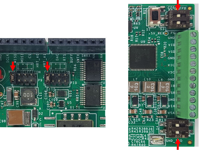
Default Shunt Jumper (P9 and P10) and DIP Switches (S3 and S4) Configuration
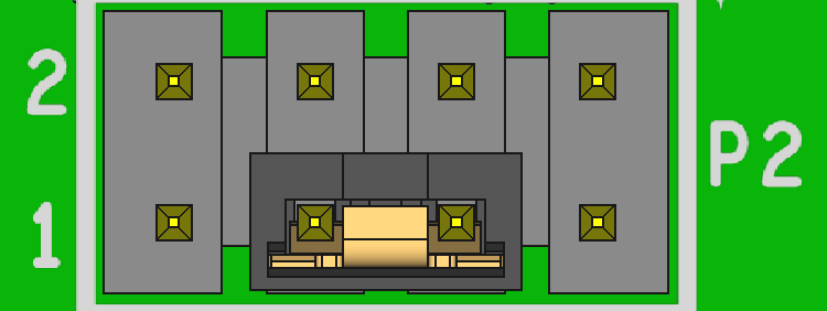
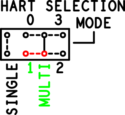
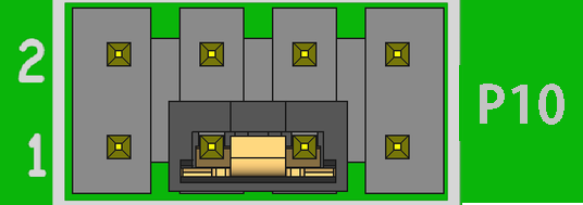
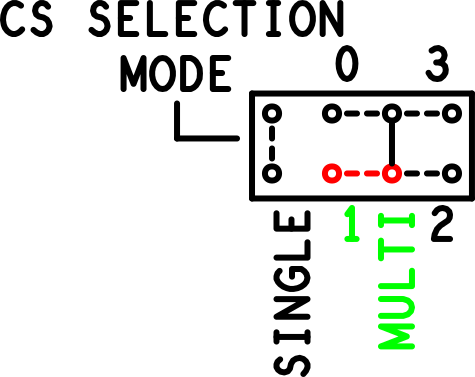
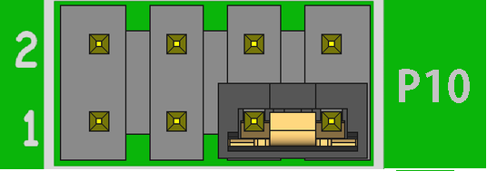
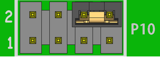
The default jumper position for P9 and P10 are shorted at position 1 and 2 while the two DIP switches S3 and S4 should be in ON state switch position.
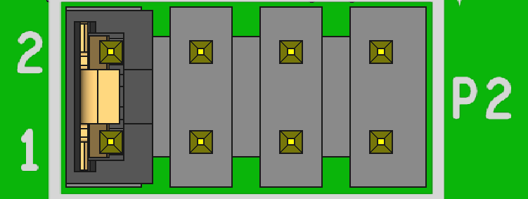
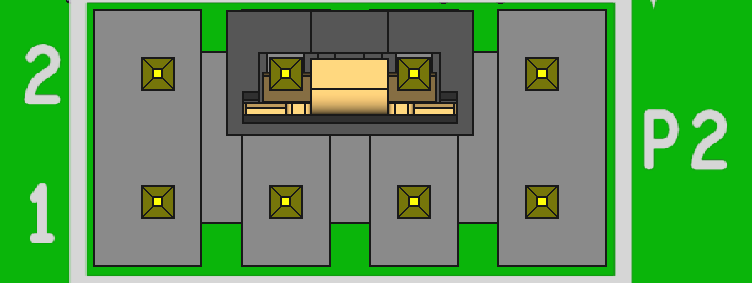
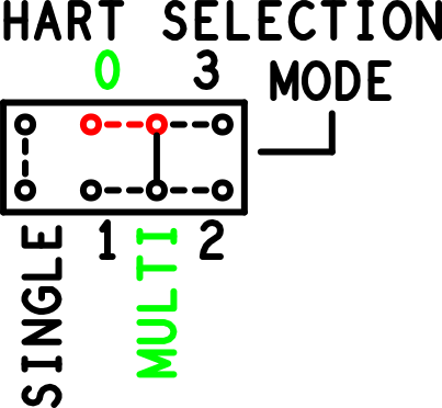
P9 jumper connections for HART enable (EN) control |
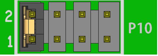
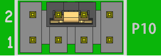
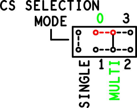
P10 jumper connections for Chip select (SYNC) control |
||||
|---|---|---|---|---|---|
Single board
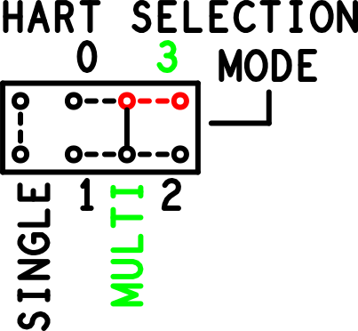
If only a single board is used, then connect jumpers P9 and P10 as shown in the table below.
Position |
Description |
Mode |
Position |
Description |
Mode |
|---|---|---|---|---|---|
pin 1 & pin 2 |
skip decoder |
single |
pin 1 & pin 2 |
skip decoder |
single |


Multi board
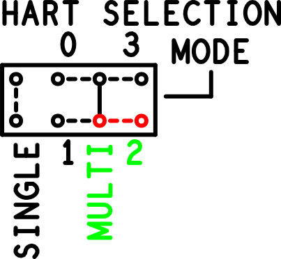
If more than one board is stacked (up to 4), then each board must be set to a different DAC and HART select address. Connect jumpers P9 and P10 as shown in the table below, and ensure that the software is configured accordingly. On a given board, set the DAC and HART address to the same position. If necessary, the software can be changed to address differently the DAC and HART on a given board.
Position |
Description |
Mode |
Position |
Description |
Mode |
|---|---|---|---|---|---|
pin 4 & pin 6 |
AIN2:AIN3 = 00 |
multiple |
pin 4 & pin 6 |
AIN0:AIN1 = 00 |
multiple |
pin 3 & pin 5 |
AIN2:AIN3 = 01 |
multiple |
pin 3 & pin 5 |
AIN0:AIN1 = 01 |
multiple |
pin 7 & pin 5 |
AIN2:AIN3 = 10 |
multiple |
pin 7 & pin 5 |
AIN0:AIN1 = 10 |
multiple |
pin 8 & pin 6 |
AIN2:AIN3 = 11 |
multiple |
pin 8 & pin 6 |
AIN0:AIN1 = 11 |
multiple |
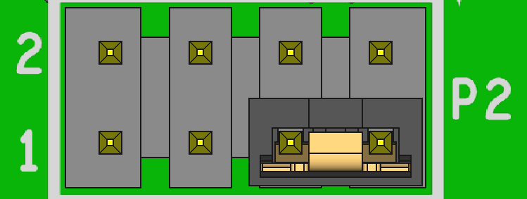

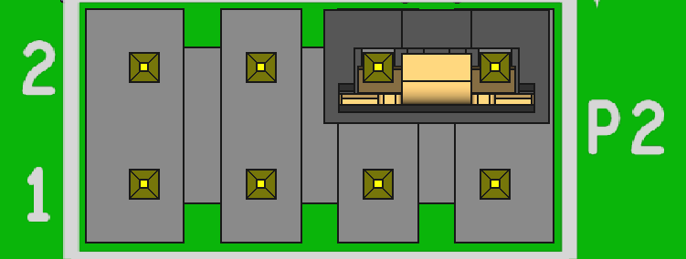

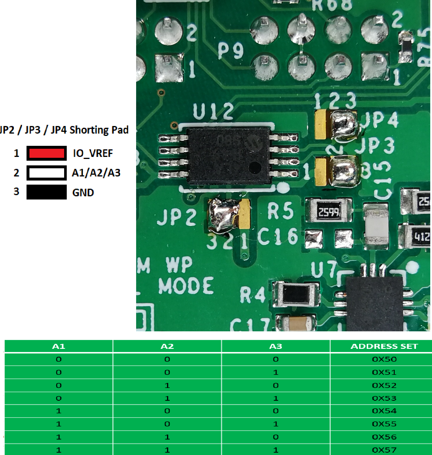
Default EEPROM Address configuration of Solder Jumper position JP2, JP3 and JP4
EEPROM default address configuration of the board is “000” you can configure the EEPROM I2C address from 000 to 111.
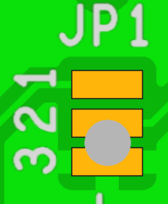
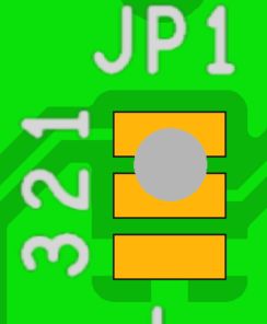
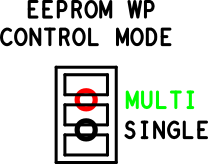
Default EEPROM WP ( Write Protect) mode configuration of Solder Jumper JP1
EEPROM WP pin can be configured as single or multi board operation. The default connection of WP pin is shorted to GND.
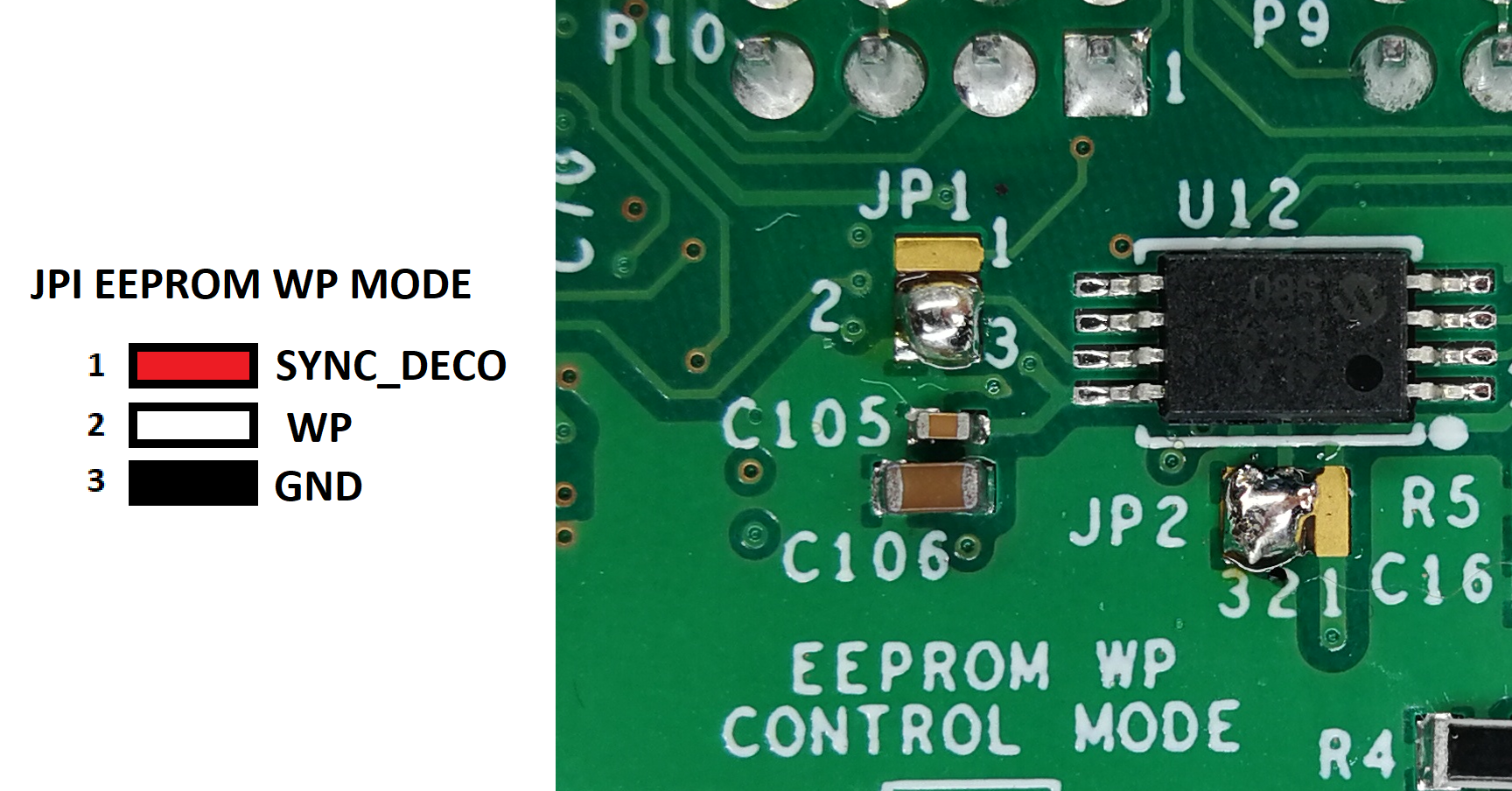
JP1 soldering position |
|
|---|---|
Position |
Description |
pin 2 & pin 3 |
enable write protection (WP) (single board operation by default) |
pin 2 & pin 1 |
control write protection (WP) (multi board operation) |

16 bit Voltage and Current Analog Output Connection (P6)
Peripheral Connectors
All connector pinouts for the EVAL-CN0418-ARDZ are described in the table below.
Connector |
Pin No. |
Pin Name |
ADuCM3029 Pin Function |
CN0418 Pin Function |
|---|---|---|---|---|
Arduino DIO High |
1 |
SCL |
I2C0_SCL/GPIO04 |
SCL (EEPROM) |
2 |
SDA |
I2C0_SDA/GPIO05 |
SDA (EEPROM) |
|
3 |
AREF |
VREF+ |
NC |
|
4 |
AGND |
AGND (Analog ground) |
DGND |
|
5 |
SCLK |
SPI0_CLK/SPT0_BCLK/GPIO00 |
DAC_SCLK (AD5755-1) |
|
6 |
MISO |
SPI0_MISO/SPT0_BD0/GPIO02 |
DAC_MISO_BUFF (AD5755-1) |
|
7 |
MOSI |
SPI0_MOSI/SPT0_BFS/GPIO01 |
DAC_MOSI (AD5755-1) |
|
8 |
CS |
SPI0_CS1/SYS_CLKIN/SPI1_CS3/GPIO26 |
DAC_SYNC(AD5755-1) |
|
9 |
RDY |
SPI0_RDY/GPIO30 |
HART_MULT_A0(AD5700-1) |
|
10 |
IO28 |
GPIO28 |
HART_MUL_A1(AD5700-1) |
|
Arduino DIO Low |
1 |
IO08 |
BPR0_TONE_N/GPIO08 |
DAC_FAULT(AD5755-1) |
2 |
IO27 |
TMR1_OUT/GPIO27 |
AD5700_RTS (AD5700-1) |
|
3 |
IO33 |
XINT0_WAKE3/TMR2_OUT/GPIO33 |
AD5700_CD_BUFF(AD5700-1) |
|
4 |
IO09 |
BPR0_TONE_P/SPI2_CS1/GPIO09 |
SW_TXD (AD5700-1) |
|
5 |
IO13 |
XINT0_WAKE2/GPIO13 |
HW RXD (AD5700-1) |
|
6 |
IO15 |
XINT0_WAKE0/GPIO15 |
NC |
|
7 |
TX |
UART0_TX/GPIO10 |
NC |
|
8 |
RX |
UART0_RX/GPIO11 |
NC |
|
Arduino Analog |
1 |
AIN0 |
ADC0_VIN0/GPIO35 |
HART_COM_A0 |
2 |
AIN1 |
ADC0_VIN1/GPIO36 |
HART_COM_A1 |
|
3 |
AIN2 |
ADC0_VIN2/GPIO37 |
DAC_COM_A0 |
|
4 |
AIN3 |
ADC0_VIN3/GPIO38 |
DAC_COM_A1 |
|
5 |
AIN4 |
ADC0_VIN4/SPI2_CS3/GPIO39 |
NC |
|
6 |
AIN5 |
ADC0_VIN5/SPI0_CS2/GPIO40 |
NC |
|
Arduino Power |
1 |
NC |
|
NC |
2 |
IOREF |
+3.3V |
IO_VREF (+3V3) |
|
3 |
RESET |
SYS_HWRST_N |
NC |
|
4 |
3.3V |
+3.3V |
NC |
|
5 |
5V |
+5V |
5V |
|
6 |
GND |
DGND (Digital Ground) |
GND |
|
7 |
GND |
DGND (Digital Ground) |
GND |
|
8 |
Vin |
DC Barrel Jack Power +7V to +12V |
+7.5V |
Advanced Setup
Up to four EVAL-CN0418-ARDZ boards can be controlled by a single Arduino or EVAL-ADICUP3029 base board by using a simple control scheme. This control scheme will control the SYNC, CD and RX signals to avoid a data conflict.
More Information and Useful Links
Schematic, PCB Layout, Bill of Materials
Download
EVAL-CN0418-ARDZ Design & Integration Files
Schematics
PCB Layout
Bill of Materials
Allegro Project
Software
Registration
Tip
Receive software update notifications, documentation updates, view the latest videos, and more when you register your hardware. Register to receive all these great benefits and more!
End of Document