EVAL-CN0414-ARDZ Shield Overview
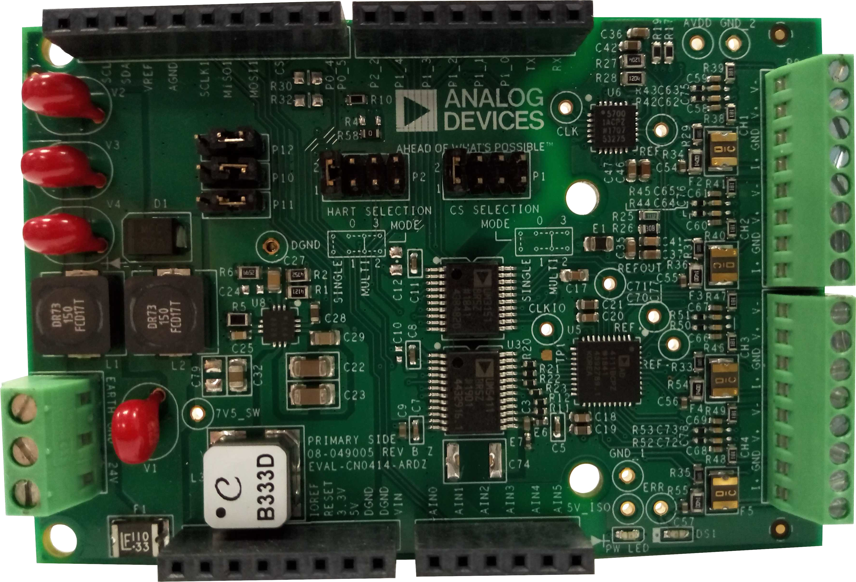
CN0414 is an Arduino compatible shield that provides a complete, fully isolated, highly flexible, quad channel analog input system suitable for programmable logic controllers (PLCs) and distributed control system (DCS) applications that require multiple voltage inputs and 4 mA to 20 mA current inputs. Additionally, the 4-20 mA inputs provide HART communication to remote field devices.
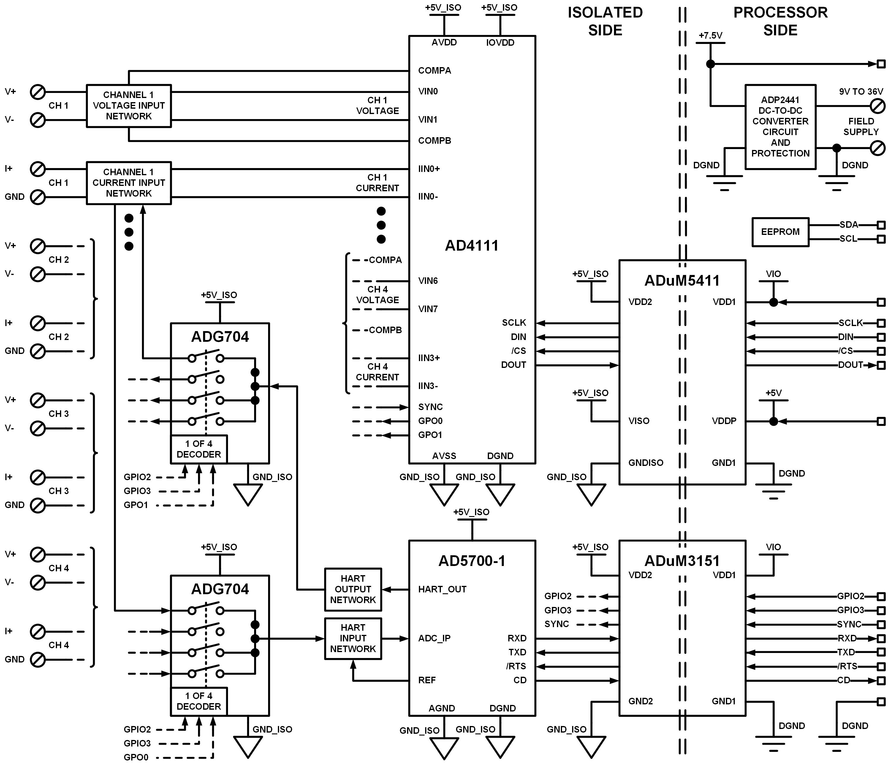
The circuit shown below uses ad4111, a low power, low noise, 24-bit, sigma-delta (Σ-Δ) analog-to-digital converter (ADC) that integrates an analog front end (AFE) for fully differential or single-ended rail-to-rail, bipolar, ±10 V voltage inputs, and 0 mA to 20 mA current inputs. The AD5700-1 is the industry’s lowest power and smallest footprint HART-compliant modem and is used in conjunction with the current input channels to form a HART-compatible, 4 mA to 20 mA receiver solution. The ADG704 multiplexer provides HART connectivity to the multiple current input channels. The ADuM5411 and ADuM3151 provide digital line and power isolation. The ADP2441 36 V, step-down, dc-to-dc regulator accepts an industrial standard 24 V supply, with wide tolerance on the input voltage and steps it down to 7.5V to be used by the system.
This user guide will discuss how to use the EVAL-EVAL-ADICUP3029 and evaluation software to configure and collect data from the EVAL-CN0414-ARDZ Evaluation Board (CN-0414 Board).
Simplified functional block diagram
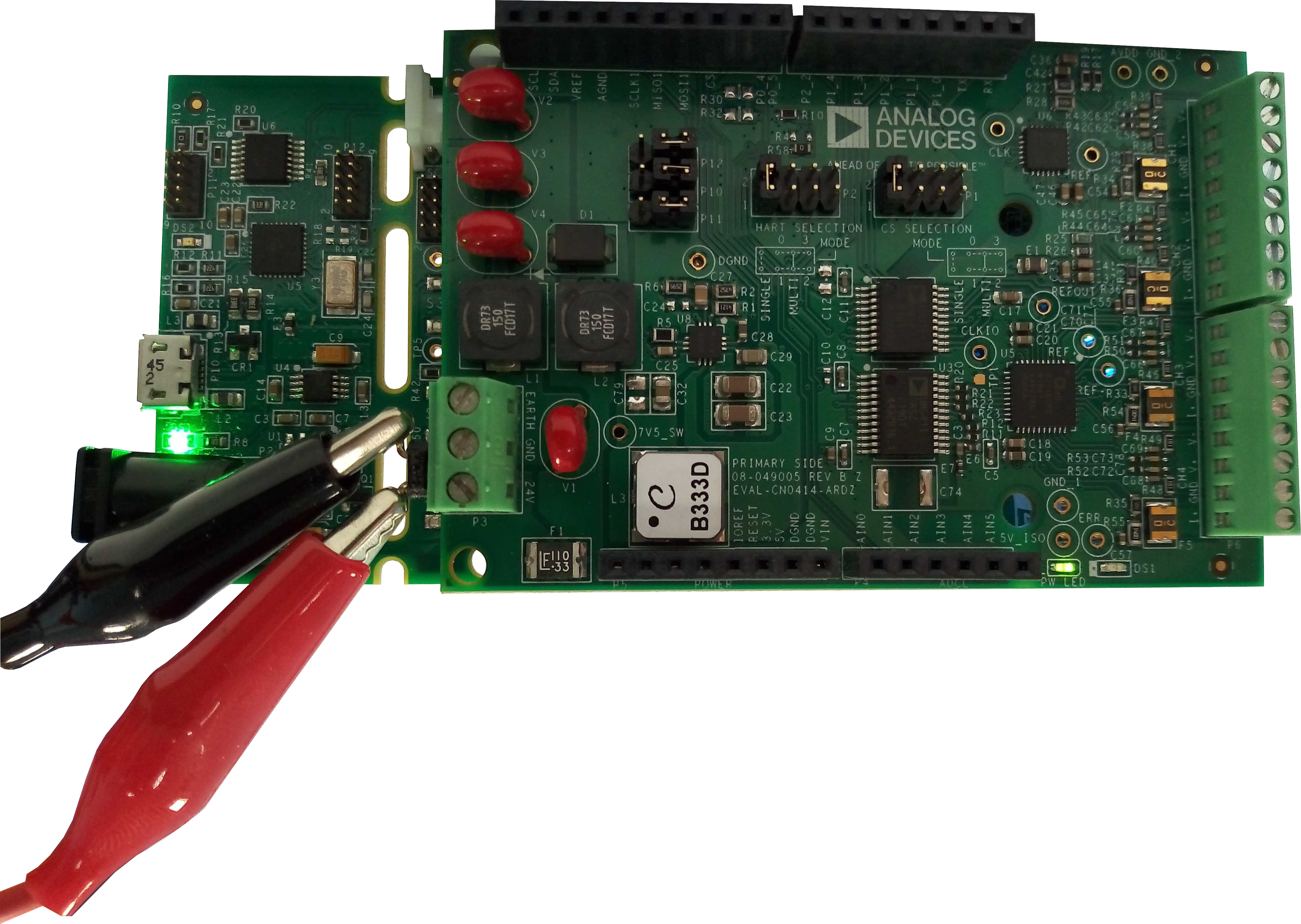
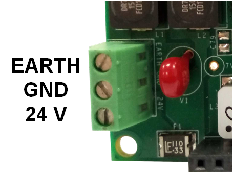
Power Supply Considerations and Configuration (P3)
Terminal block P3 is the power supply input (input range:+9.5V to +36V DC). The EARTH terminal can be connected to an external earth connection, to the GND terminal or left floating if an external earth connection is not used.
Main power setup |
P3 terminals description |
|---|---|
|
|
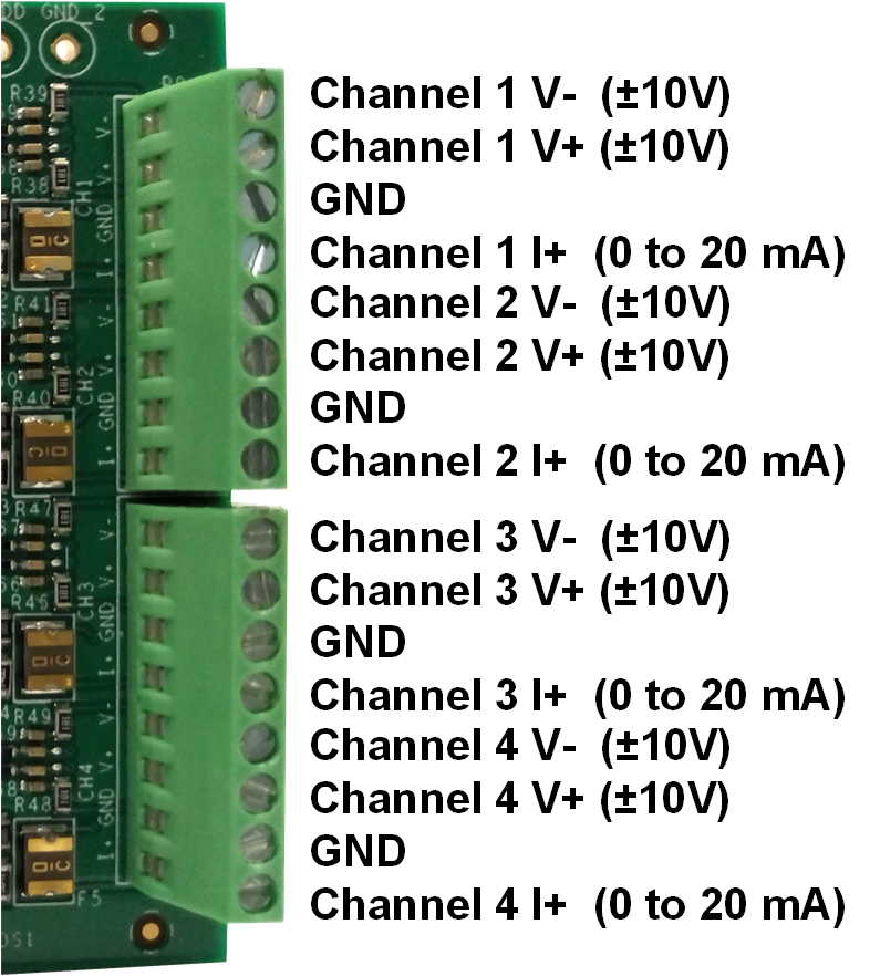
Analog Input Connections (P6 and P9)
The analog input circuit is designed for group-isolated industrial analog inputs and can support voltage and current inputs in the following ranges:
Range |
Analog Input Terminals Description |
|---|---|
|
|
|
|
|
|
|
|
|
|
|
|
|
Single Board
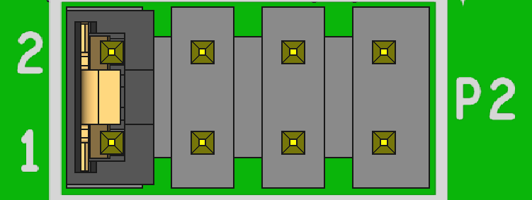
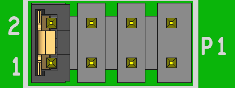
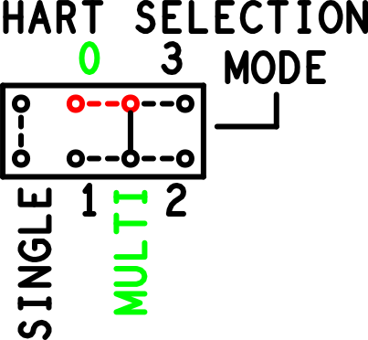
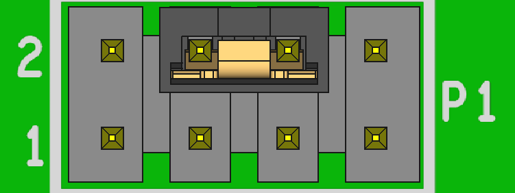
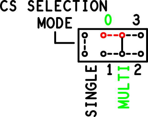
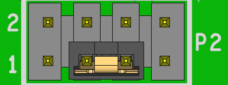
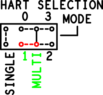
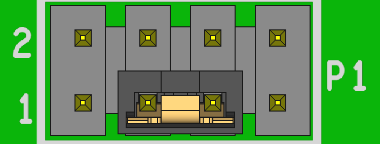
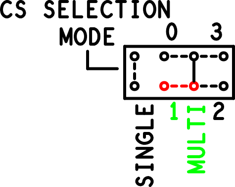
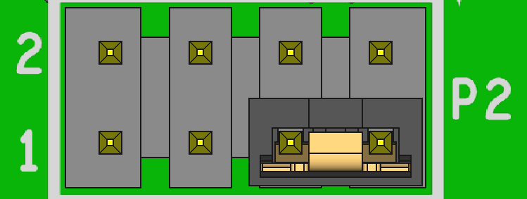
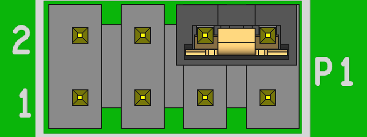
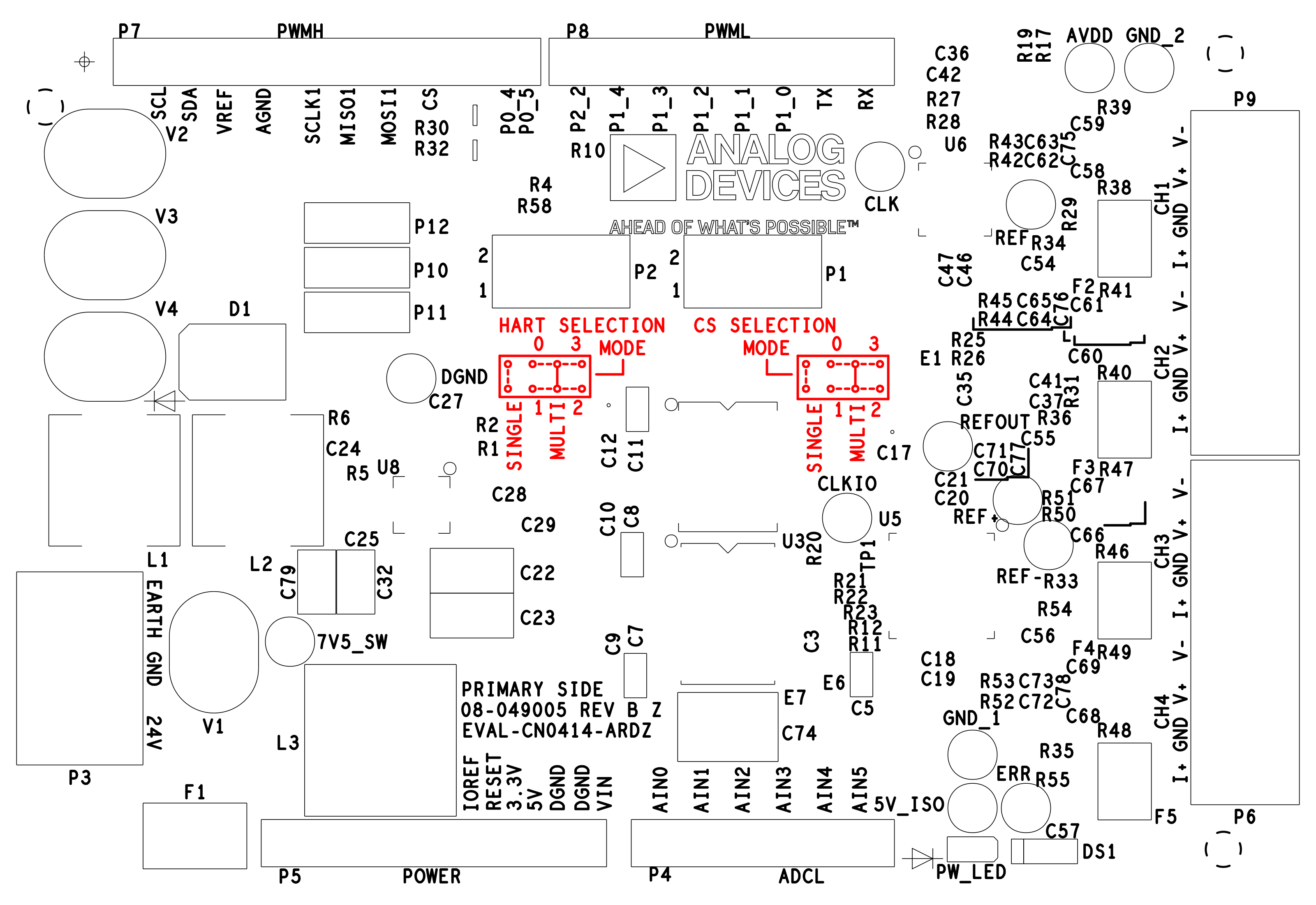
If only a single board is used, then connect jumpers P1 and P2 as shown in the table below.
P2 Jumper Connections |
P1 Jumper Connections |
||||
|---|---|---|---|---|---|
Position |
Description |
Mode |
Position |
Description |
Mode |
pin 1 & pin 2 |
skip decoder |
single |
pin 1 & pin 2 |
skip decoder |
single |


Multiple Boards Stacked
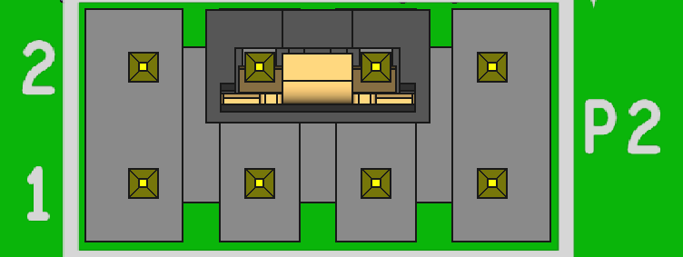
If more than one board is stacked (up to 4), then each board must be set to a different ADC and HART select address. Connect jumpers P1 and P2 as shown in the table below, and ensure that the software is configured accordingly. On a given board, set the ADC and HART address to the same position. If necessary, the software can be changed to address differently the ADC and HART on a given board.
P2 Jumper Connections |
P1 Jumper Connections |
||||
|---|---|---|---|---|---|
Position |
Description |
Mode |
Position |
Description |
Mode |
pin 4 & pin 6 |
AIN2:AIN3 = 00 |
multiple |
pin 4 & pin 6 |
AIN0:AIN1 = 00 |
multiple |
pin 3 & pin 5 |
AIN2:AIN3 = 01 |
multiple |
pin 3 & pin 5 |
AIN0:AIN1 = 01 |
multiple |
pin 7 & pin 5 |
AIN2:AIN3 = 10 |
multiple |
pin 7 & pin 5 |
AIN0:AIN1 = 10 |
multiple |
pin 8 & pin 6 |
AIN2:AIN3 = 11 |
multiple |
pin 8 & pin 6 |
AIN0:AIN1 = 11 |
multiple |
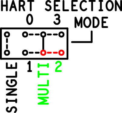
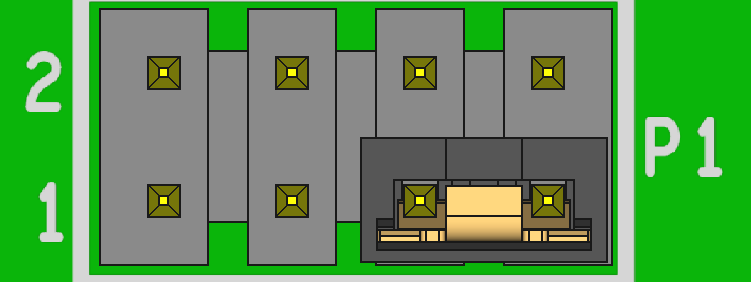

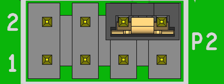
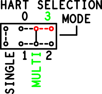

EEPROM Address Configurations
For multiple boards configuration, it is mandatory to set a different EEPROM address for each board. In this way, on software initialization, the system configuration (how many boards, what type and at what address) will be determined.
EEPROM address selection |
|||
|---|---|---|---|
P10 jumper position |
P11 jumper position |
P12 jumper position |
Address set |
pin 2 & pin 3 |
pin 2 & pin 3 |
pin 2 & pin 3 |
0x50 |
pin 2 & pin 1 |
pin 2 & pin 3 |
pin 2 & pin 3 |
0x51 |
pin 2 & pin 3 |
pin 2 & pin 1 |
pin 2 & pin 3 |
0x52 |
pin 2 & pin 1 |
pin 2 & pin 1 |
pin 2 & pin 3 |
0x53 |
pin 2 & pin 3 |
pin 2 & pin 3 |
pin 2 & pin 1 |
0x54 |
pin 2 & pin 1 |
pin 2 & pin 3 |
pin 2 & pin 1 |
0x55 |
pin 2 & pin 3 |
pin 2 & pin 1 |
pin 2 & pin 1 |
0x56 |
pin 2 & pin 1 |
pin 2 & pin 1 |
pin 2 & pin 1 |
0x57 |
EEPROM Configuration for Single or Multiple Boards configuration (JP1)
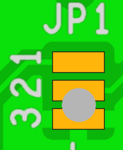
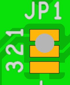
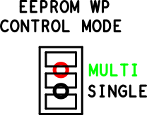
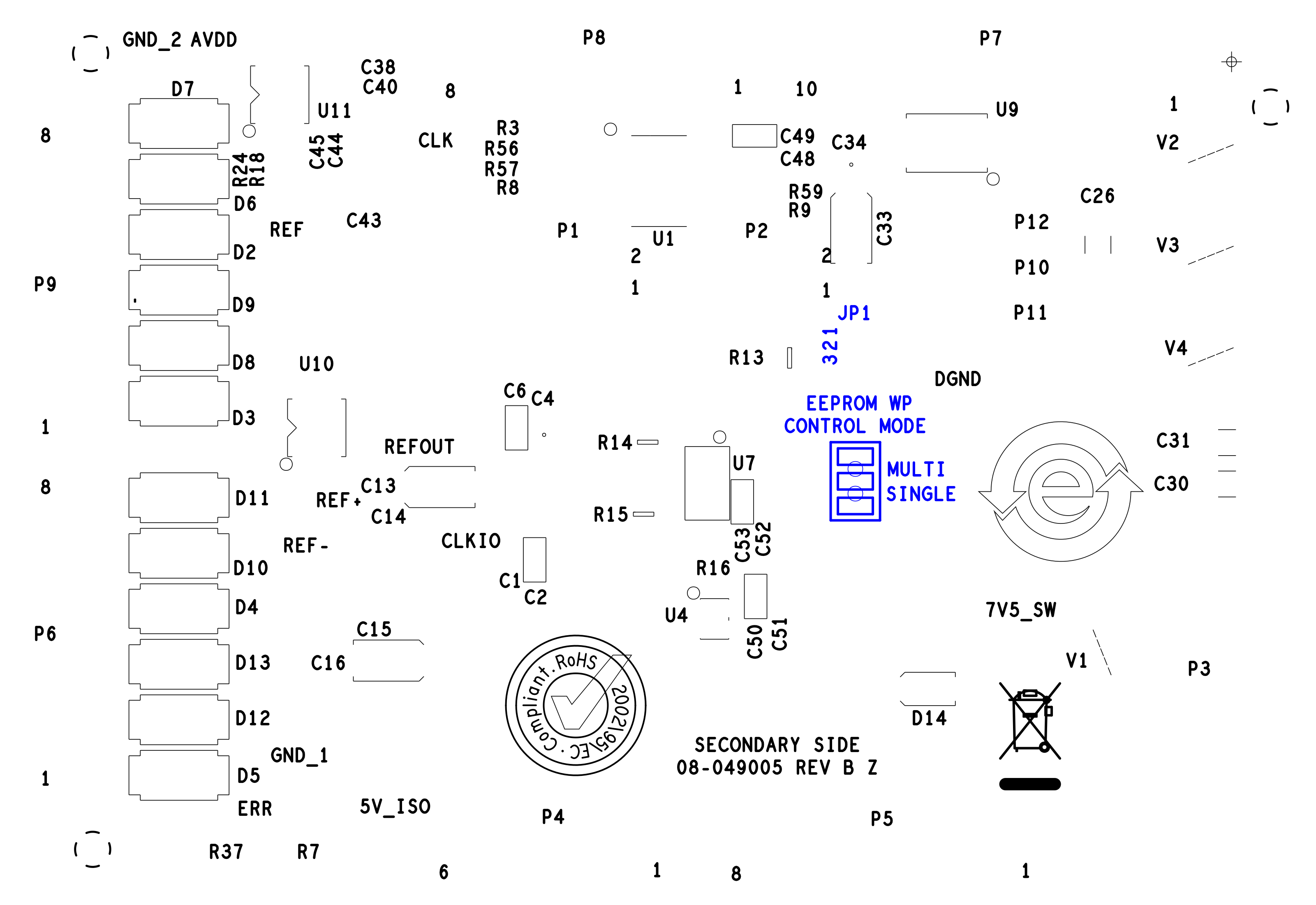
If only a single board is being used, then ensure that JP1 Solder Jumper is shorting pins 2 & 3 as shown in the table below. If multiple boards are used, short pins 1 & 2.
JP1 soldering position |
|
|---|---|
Position |
Description |
pin 2 & pin 3 |
enable write protection (WP) (single board operation) |
(default) |
|
pin 2 & pin 1 |
disable write protection (WP) (multi board operation) |

LED Indicators
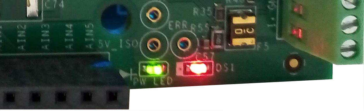
There are two LEDs on the board. The power LED is on as time the board is powered. The error LED is off by default.
More Information and Useful Links
Schematic, PCB Layout, Bill of Materials
Download
EVAL-CN0414-ARDZ Design & Integration Files
Schematics
PCB Layout
Bill of Materials
Allegro Project
Software
Registration
Tip
Receive software update notifications, documentation updates, view the latest videos, and more when you register your hardware. Register to receive all these great benefits and more!
End of Document