AD-PZSDR2400TDD-EB Hardware

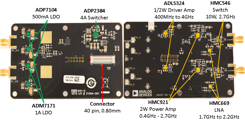
Picture and Main Components
https://media.githubusercontent.com/media/analogdevicesinc/system-level/main/docs/solutions/reference-designs/ad-pzsdr2400tdd-eb/images/parts_list.png

Figure 1 AD-PZSDR2400TDD-EB main components.

Outline

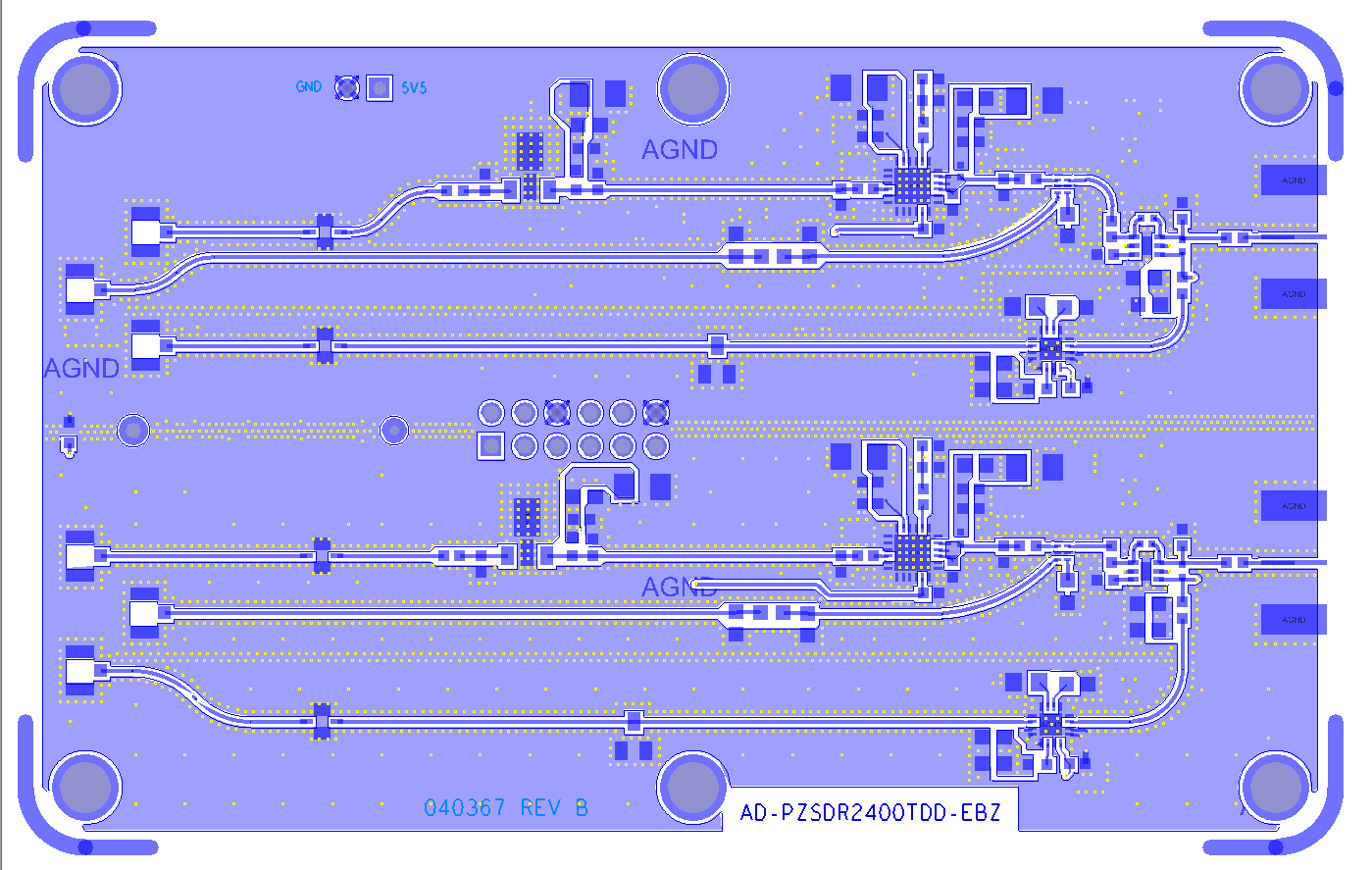
For those that don’t want to load up the Allegro viewer, here is a basic outline/component placements of the board. The PCB measures 100mm x 62mm and is the same form factor as the RFSOM.
https://media.githubusercontent.com/media/analogdevicesinc/system-level/main/docs/solutions/reference-designs/ad-pzsdr2400tdd-eb/images/top_copper_top_overlay.png

Figure 2 Top copper and top overlay.

Size

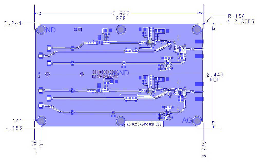
The size of the board (not including the SMA connectors, which project beyond the edge of the board) is 100mm x 62mm. The mounting holes align with the carrier card (AES-PZSDRCC-FMC-G), and are shown below.
https://media.githubusercontent.com/media/analogdevicesinc/system-level/main/docs/solutions/reference-designs/ad-pzsdr2400tdd-eb/images/pcb_dimensions.png

Figure 3 PCB dimensions.

Layers

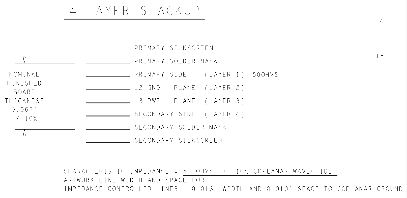
The AD-PZSDR2400TDD-EB is a 4 layer board.
https://media.githubusercontent.com/media/analogdevicesinc/system-level/main/docs/solutions/reference-designs/ad-pzsdr2400tdd-eb/images/layer_stackup_2.png

Figure 4 Layer stackup.