ADRV904x HDL reference design
Important
We are in the process of migrating our documentation to GitHubIO. This page is outdated and the new one can be found at https://analogdevicesinc.github.io/hdl/projects/adrv904x/index.html
The reference design supports the following evaluation board:
Supported Carriers
ZCU102 FMC0 Slot
Building the HDL project
General build instructions can be found here: Building HDL
Block Diagram
The data path and clock domains are depicted on the below diagram:
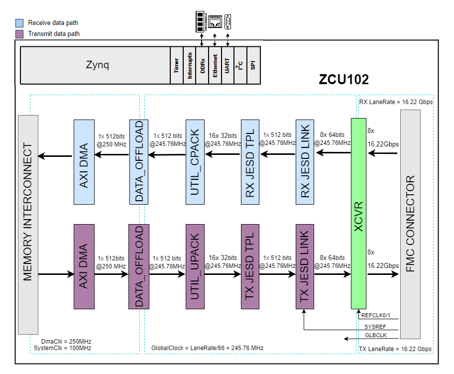
The Rx links (ADC Path) operate with the following parameters:
Rx Deframer parameters: L=8, M=16, F=4, S=1, N’=16, N=16
Sample Rate : 491.52 MSPS
RX_DEVICE_CLK – 245.76 MHz (Lane Rate/66)
REF_CLK – 491.52 MHz (Lane Rate/33)
JESD204C Lane Rate – 16.22 Gbps
QPLL0
The Tx links (DAC Path) operate with the following parameters:
Tx Framer parameters: L=8, M=16, F=4, S=1, N’=16, N=16
Sample Rate : 491.52 MSPS
TX_DEVICE_CLK – 245.76 MHz (Lane Rate/66)
REF_CLK – 491.52 MHz (Lane Rate/33)
JESD204C Lane Rate – 16.22 Gbps
QPLL0
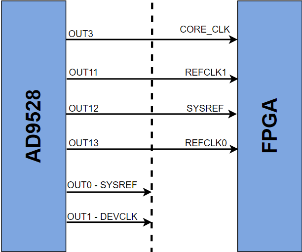
Clock sources
The clock sources are depicted on the below diagram:
More Information
Support
Analog Devices will provide limited online support for anyone using the core with Analog Devices components (ADC, DAC, Video, Audio, etc) via the EngineerZone.