User guide
Hardware guide
Hardware configuration
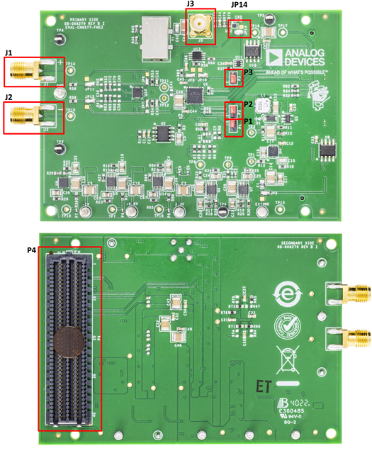
Connector Name |
Operation |
Description |
Settings/Ranges |
P1 |
Power Down (PD) Mode |
When PD is high CN0577 will operate normally, but when PD is low CN0577 board enters power-down mode and all circuitry (including LVDS interface) is shutdown. |
PD = High (Pins 1 and 2) |
PD = Low (Pins 2 and 3) |
|||
P2 |
Test Pattern (TESTPAT) |
Forces the LVDS data outputs to be a test pattern. When TESTPAT is high digital outputs are a test pattern, and when TESTPAT is low digital outputs are the ADC conversion result. |
TESTPAT = High (Pins 1 and 2) TESTPAT = Low (Pins 2 and 3) |
P3 |
Lane Mode Selection |
The ADC outputs two bits at a time on DA-/DA+ and DB-/DB+ when two-lane output mode is high, and the ADC outputs one bit at a time on DA-/DA+ and DB-/DB+ when two-lane output mode is low. |
TWOLANES = High (Pins 1 and 2) |
TWOLANES = Low (Pins 2 and 3) |
|||
P4 |
FMC Connector (LPC) |
Low pin count FMC connector used to connect the EVAL-CN0577-FMCZ hardware to various different FPGA development boards and kits. |
N/A |
J1 |
Positive Analog Input |
This is the positive input to the EVAL-CN0577-FMCZ, which connects to external signal sources via an SMA connection. |
0V to 4.096 V |
J2 |
Negative Analog Input |
This is the negative input to the EVAL-CN0577-FMCZ, which connects to external signal sources via an SMA connection. |
0V to -4.096 V |
J3 |
External Clock |
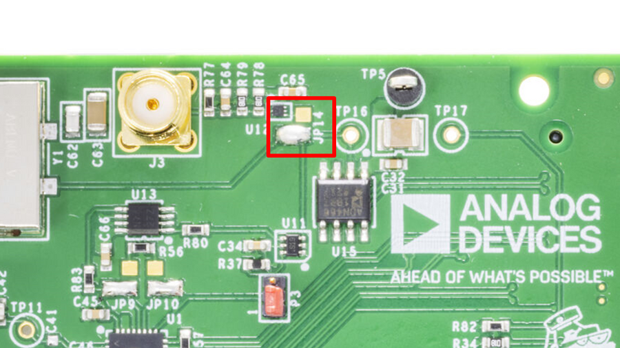
If an external clocking source is desired in your system this is where you will need to connect it. Along with connecting it you will also need to update the solder jumper (JP14) to change from the onboard crystal oscillator. |
On-board Crystal Oscillator (default 120 MHz) |
JP14 |
External source (120 MHz desired) |
||
Power supply
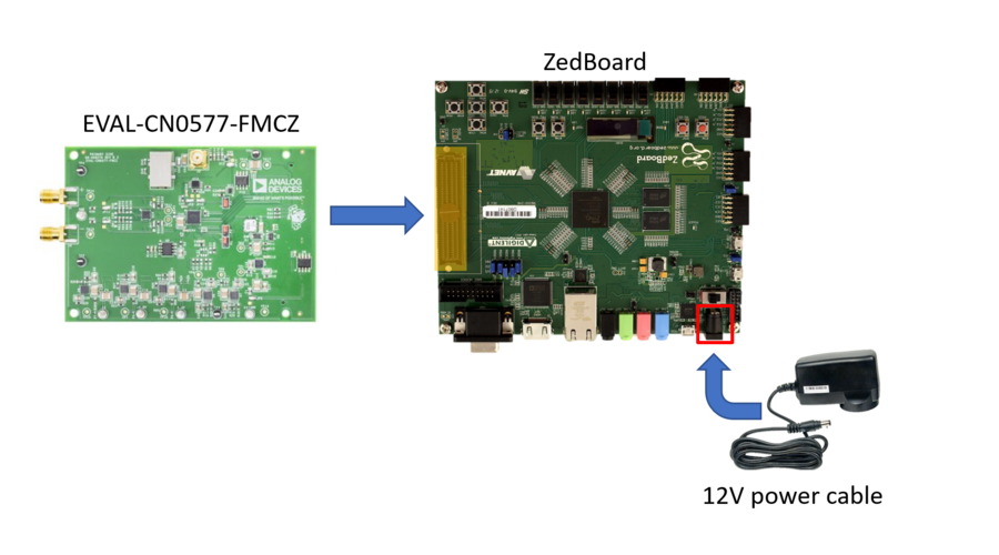
Power to the EVAL-CN0577-FMCZ comes directly from the +12 V supply provided through the FMC connector.
Analog inputs
The SMA connectors on the EVAL-CN0577-FMCZ (VIN+ and VIN−) provide analog inputs from a low noise, audio precision signal source (such as the Audio Precision audio analyzer).
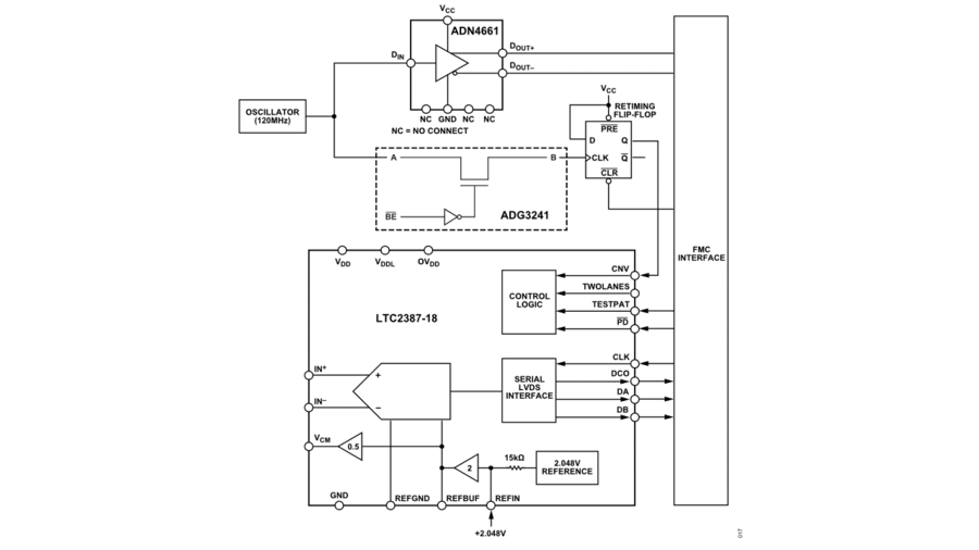
Onboard clock reference
The EVAL-CN0577-FMCZ clock diagram is shown in the figure below. An onboard 120 MHz voltage controlled crystal oscillator is used to provide the clock for the EVAL-CN0577-FMCZ and the FPGA. This ultralow noise oscillator has a typical phase noise of -162 dBc/Hz at 10 kHz offset, a tuning voltage range of 0 V to 3.3 V, and a frequency pulling range of 28 ppm to 55 ppm. Additionally, this crystal oscillator has an RMS jitter of <50 fs to 100 fs at 100 MHz carrier.
The clock is fanned out to the retiming flip-flop and the FPGA. An ADG3241 level shifter converts the clock’s 3.3 V logic level to the 2.5 V level required by the retiming flip-flop. An ADN4661 converts the 3.3 V clock to LVDS signaling, which is then forwarded to a global clock connection on the FMC connector.
External clock reference option
If the EVAL-CN0577-FMCZ is to be synchronized to other circuits, or if tighter frequency accuracy or drift is required, an external clock can be applied to the external clock connector (J3). Along with connecting it, you will also need to update the solder jumper (JP14) to change from the onboard crystal oscillator. If the external clock frequency is significantly higher or lower than the on-board 120 MHz clock, reanalyze the entire circuit including the FPGA timing constraints.
The external clock circuitry also includes a high speed single inverter that provides AC coupling and balances the rise and fall times. This device has a typical time propagation delay of 2.4 ns and achieves a high output drive, while maintaining low static power dissipation over a broad VCC operating range.
Schematic, PCB Layout, Bill of Materials
Download
EVAL-CN0577-FMCZ Design & Integration Files
Schematics
PCB Layout
Bill of Materials
Allegro Project
LTspice Simulation File
Software guide
The EVAL-CN0577-FMCZ is supported with the Libiio library. This library is cross-platform (Windows, Linux, Mac) with language bindings for C, C#, Python, MATLAB, and others. Two easy examples that can be used with the EVAL-CN0577-FMCZ are:
Connection
To be able to connect your device, the software must be able to create a context. The context creation in the software depends on the backend used to connect to the device as well as the platform where the EVAL-CN0577-FMCZ is attached. The platform currently supported for the CN0577 is the ZedBoard through the ADI Kuiper Linux. The user needs to supply a URI which will be used in the context creation. The Libiio is a library for interfacing with IIO devices.
Install the Libiio package on your machine.
The iio_info command is a part of the libIIO package that reports all IIO attributes. Upon installation, simply enter the command on the terminal command line to access it.
For Windows machine connected to ZedBoard via Ethernet cable
Using SSH Terminal Software:
Open SSH Terminal Software (PuTTY, TeraTerm or similar). User should now start the PuTTY application and enter certain values in the configuration window. In the terminal, run:
user@analog:~$
iio_info -u ip:<ip_address>
Using Command Terminal:
~$
iio_info -s
Prompting this on the command terminal in your windows PC will give you the ip address to access the EVAL-CN0577-FMCZ.
~$
ssh analog@<ip_address>
user@analog:~$
iio_info -u ip:<ip_address>
IIO Commands
There are different commands that can be used to manage the device being used. The iio_attr command reads and writes IIO attributes.
~$
iio_attr [OPTION]...
Example:
To look at the context attributes, enter this code on the terminal:
~$
iio_attr -a -C
IIO Oscilloscope
Download
Make sure to download/update to the latest version of IIO Oscilloscope at ADI IIO Oscilloscope repository (releases)
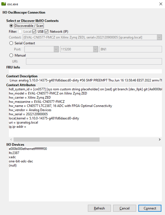
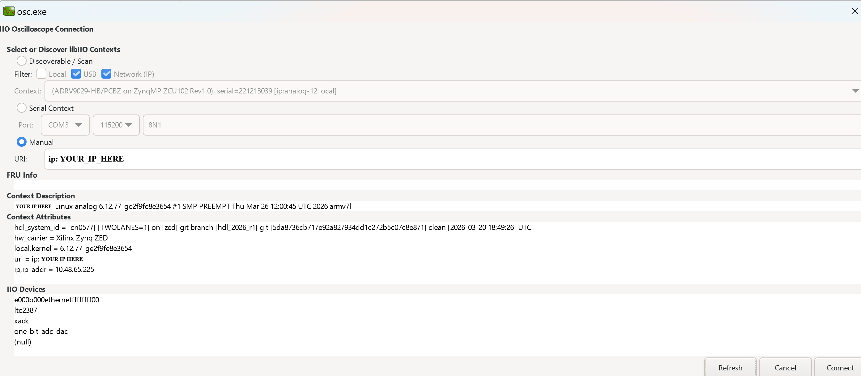
Once done with the installation or an update of the latest IIO Oscilloscope, open the application. You can either use the automatic scan to discover available devices on the network, or manually enter the URI (
ip:<ip_address>) if you already know the ZedBoard’s IP address.Press refresh to display available IIO Devices, once ltc2387 appeared, press connect.
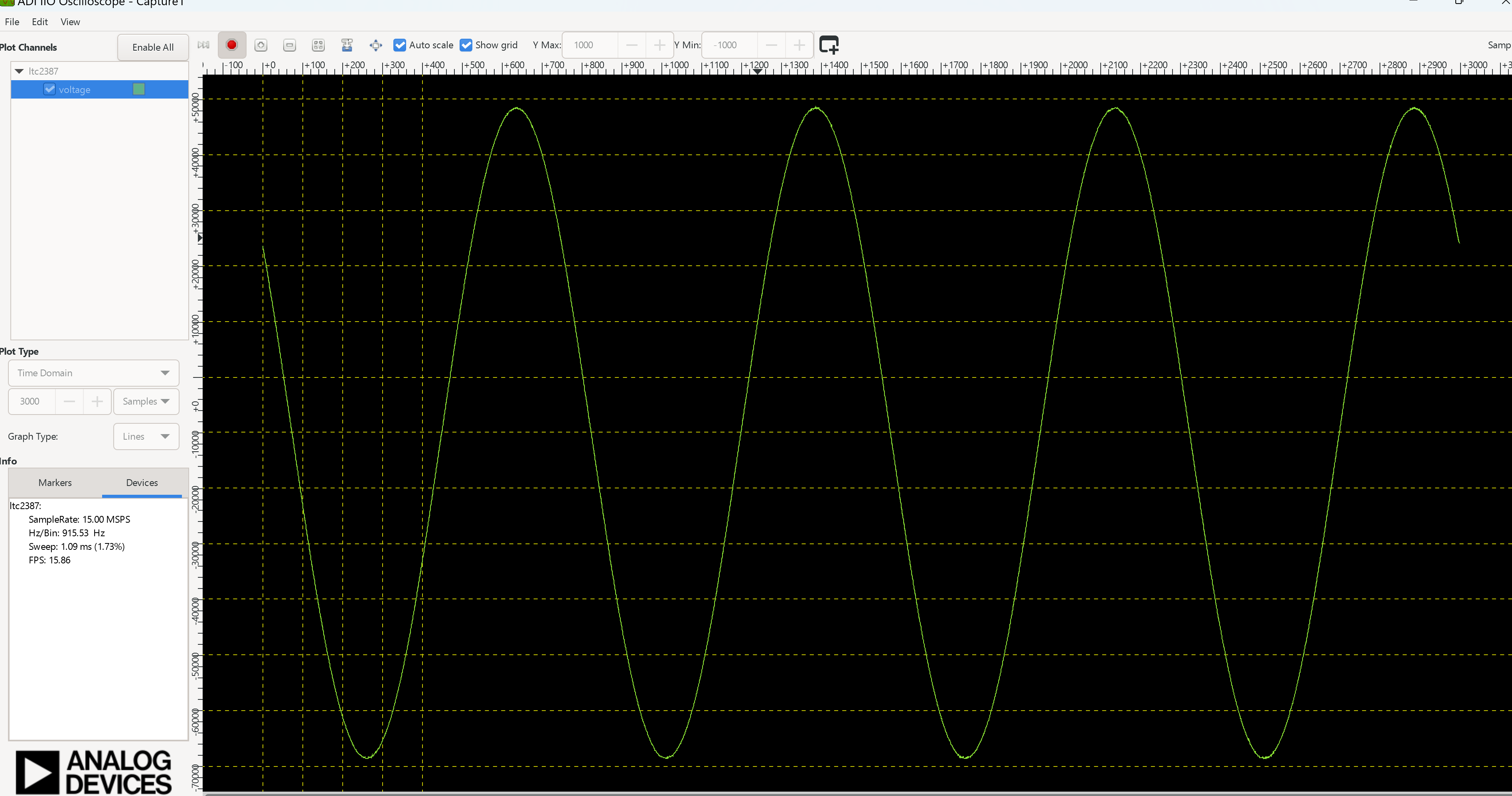
After the board is connected and a channel is enabled, hit the play button. The data capture window will display the sampled data.
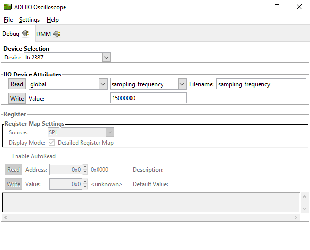
Debug Panel
Below is the Debug panel of ltc2387 wherein you can directly access the attributes of the device.
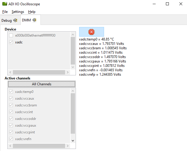
DMM Panel
Access the DMM panel to see the instantaneous reading of the ADC voltages and the device temperature.
Pyadi-IIO
PyADI-IIO is a python abstraction module for ADI hardware with IIO drivers to make them easier to use.
This module provides device-specific APIs built on top of the current libIIO python bindings. These interfaces try to match the driver naming as much as possible without the need to understand the complexities of libIIO and IIO.
Running the Example
After installing and configuring PYADI-IIO in your machine, you are now ready to run python script examples. In our case, run the ltc2387_example.py found in the examples folder.
Connect the EVAL-CN0577-FMCZ to the ZedBoard.
Open command prompt or terminal and navigate through the examples folder inside the downloaded or cloned pyadi-iio directory.
Run the example script using the command.
/path/to/pyadi-iio/examples$
python3 ltc2387_example.py
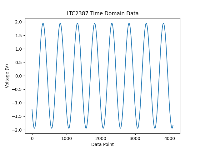
Running example with ADALM2000 with the setting below:
The expected output should look like this:
GitHub link for the python sample script: CN0577 Python Example