Hardware User Guide
The AD-IMP2501DBZ-SL and AD-IMP2501EBZ-SL are designed for evaluating impedance analysis technology in an application that requires a small form factor and wide frequency range. This platform is designed to get an impedance analysis evaluation set-up running quickly with only a provided USB cable and a computer. This hardware guide will walk the user through the basic setup, the varying jumper configurations for different measurement modes, and how to interface with an external load that is more specific to his or her application.
Equipment Needed
Required Equipment
AD-IMP2501DBZ-SL
AD-IMP2501EBZ-SL
USB C Cable
PC
USB drivers and terminal emulator required. Please see Software User Guide for instructions to download and install on your PC if not already installed.
Optional Equipment
Programming equipment for Firmware Updates
MAX32625PICO2 with ribbon cable
Impedance measurement accessories. Available from various test and measurement manufacturers. The test fixture accessories noted here would require a connector adapter.
Calibration Standards and Accessories
LCR Meter for verification
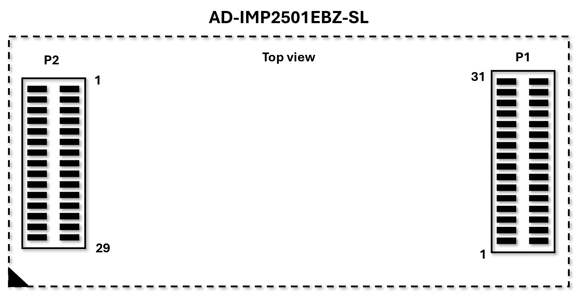
AD-IMP2501DBZ-SL Pin Configuration and Descriptions
Pin Number |
Mnemonic |
Description |
|---|---|---|
P1.1, P1.2, P1.7, P1.8,
P1.17, P1.22, P1.28,
P1.31, P1.32
|
AGND |
Ground |
P1.3 |
L_CUR |
Low Current signal |
P1.4 |
L_POT |
Voltage measurement low potential terminal |
P1.5 |
H_CUR |
High Current or signal |
P1.6 |
H_POT |
Voltage measurement high potential terminal |
P1.9 |
SQWOUT |
Square-Wave Output |
P1.10 |
TX_OUT_SELECT |
Drive Mode Select |
P1.11 |
CAN0B_RX |
Controller Area Network Receive Input |
P1.12, P1.15, P1.16,
P1.18, P1.20, P1.21,
P1.23, P1.24
|
GPIO |
General Purpose Input Output |
P1.13 |
CAN0B_TX |
Controller Area Network Transmit Output |
P1.14 |
OWM_IO |
1-Wire Controller Data |
P1.19 |
OWM_PE |
1-Wire Controller Pull-up Enable |
P1.25 |
ST_ENABLE |
Self-Test Enabled |
P1.26 |
OUTPUT_ENABLE |
CSignal Output Enabled |
P1.27 |
ST_ENABLE_N |
Self-Test Not Enabled |
P1.29 |
MCU_RESET_N |
Active-Low. External System Reset Input |
P1.30 |
PDOWN |
Power-Down Output |
P2.1 |
I2C_SCL |
I2C Serial Clock |
P2.2 |
SPI2A_SCK |
SPI Clock |
P2.3 |
I2C_SDA |
I2C Serail Data |
P2.4 |
SPI2A_CITO |
SPI Controller In Target Out |
P2.5 |
POWER_GOOD |
Power Boot-up Verification Signal |
P2.6 |
SPI2A_SDIO2 |
SPI Data 2 |
P2.7, P2.13, P2.14,
P2.20, P2.21, P2.27,
P2.28
|
AGND |
Ground |
P2.8 |
SPI2A_COTI |
SPI Controller Out Target In |
P2.9 |
UART_RX |
UART Receive |
P2.10 |
SPI2B_SDIO3 |
SPI Data 3 |
P2.11 |
UART_TX |
UART Transmit |
P2.12 |
SPI2A_SS0 |
SPI Target Select 0 |
P2.15 |
SPI2A_SS1 |
SPI Target Select 1 |
P2.16 |
SWDIO |
Serial Wire Debug I/O |
P2.17 |
USBC_DM |
USBC Differential pair D- |
P2.18 |
SWDCLK |
Serial Wire Debug Clock |
P2.19 |
USBC_DP |
USBC Differential pair D+ |
P2.22 |
VDD_3P3_D |
+3.3V Digital Rail output from AD-IMP2501DBZ-SL |
P2.23 |
VDD_3P3_A |
+3.3V Analog Rail output from AD-IMP2501DBZ-SL |
P2.24 |
VDD_1P8 |
+1.8V Rail output from AD-IMP2501DBZ-SL |
P2.25 |
VCC |
+5V Rail output from AD-IMP2501DBZ-SL |
P2.26 |
VEE |
-5V Rail output from AD-IMP2501DBZ-SL |
P2.29, P2.30 |
FC_VPOWER_IN |
Input Power Supply for AD-IMP2501DBZ-SL (+5V nominal) |
All Other Pins |
DNC |
Do Not Connect |
General Setup
The following figure shows the basic connections required for evaluating the ADMX2501B.
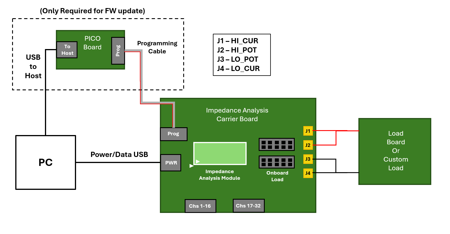
Insert the AD-IMP2501DBZ-SL module into the AD-IMP2501EBZ-SL board in the location shown above. Use the small white triangle on both the module and the carrier board to orient properly. The connectors are different sizes, so they can only be inserted in one orientation shown, but excessive force in the wrong orientation could damage the connectors.
Use the picture below and the following tables to install the correct jumpers for your desired operation. The first table is for power and general communication. The second table is for EIS on board measurements. The third table is for EIS off board measurements.
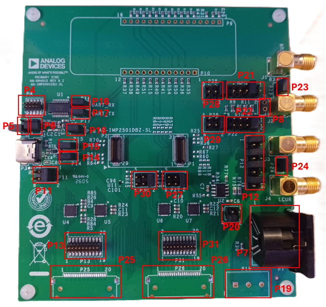
Verify jumpers are installed in the locations designated by the following table for power and communication.
Jumper Designation |
Install Position |
Description |
|---|---|---|
P4 |
Not Installed |
Programming Header |
P5 |
Not Installed |
Debug UART RX |
P6 |
Not Installed |
Debug UART TX |
P11 |
Pins 1-2 |
USB C Power Supply |
P14 |
Pins 1-2 |
USB C DM |
P15 |
Pins 1-2 |
USB C DP |
P16 |
Pins 1-2 |
FTDI UART RX |
P17 |
Pins 1-2 |
FTDI UART TX |
P18 |
Pins 1-2 |
FTDI Power |
P20 |
Not Installed |
CAN Bus |
For EIS on board measurements install jumpers according to the following table. Note that to select an onboard load, both jumpers, corresponding to the appropriate load, need to be installed. If the user selects their own component in position 8, no jumpers should be installed on P21 or P22.
Jumper Designation |
Install Position |
Description |
|---|---|---|
P27 |
Pins 1-2 |
EIS HCUR |
P28 |
Pins 1-2 |
EIS HPOT |
P29 |
Pins 1-2 |
EIS LPOT |
P30 |
Pins 1-2 |
EIS LCUR |
P23 |
Pins 1-2 |
HCUR to HPOT connection |
P24 |
Pins 1-2 |
LCUR to LPOT connection |
P21 |
Selectable
Pins 1-2
Pins 3-4
Pins 5-6
Pins 7-8
Pins 9-10
|
10k ohms
1k ohms
100 ohms
10 ohms
0 ohms
|
P22 |
Selectable
Pins 1-2
Pins 3-4
Pins 5-6
Pins 7-8
Pins 9-10
|
10k ohms
1k ohms
100 ohms
10 ohms
0 ohms
|
P8 |
Not Installed |
User Selectable Load |
P12 |
Pins 1-2
Pins 5-6
Pins 9-10
Pins 13-14
|
EIS HCUR SMA/Onboard
EIS HPOT SMA/Onboard
EIS LPOT SMA/Onboard
EIS LCUR SMA/Onboard
|
For EIS off board measurements using the SMA connectors, install jumpers according to the following table. Connect SMA cables to J1-J4, and verify no jumpers are installed on P8, P21, P22, P23, and P24.
Jumper Designation |
Install Position |
Description |
|---|---|---|
P27 |
Pins 1-2 |
EIS HCUR |
P28 |
Pins 1-2 |
EIS HPOT |
P29 |
Pins 1-2 |
EIS LPOT |
P30 |
Pins 1-2 |
EIS LCUR |
P23 |
Not Installed |
HCUR to HPOT connection |
P24 |
Not Installed |
LCUR to LPOT connection |
P21 |
Not Installed |
10k ohms
1k ohms
100 ohms
10 ohms
0 ohms
|
P22 |
Not Installed |
10k ohms
1k ohms
100 ohms
10 ohms
0 ohms
|
P8 |
Not Installed |
User Selectable Load |
P12 |
Pins 1-2
Pins 5-6
Pins 9-10
Pins 13-14
|
EIS HCUR SMA/Onboard
EIS HPOT SMA/Onboard
EIS LPOT SMA/Onboard
EIS LCUR SMA/Onboard
|
For EIS off board measurements using the DIN connector, only change jumpers on P12 according to the following table. Connect DIN cable to P7.
Jumper Designation |
Install Position |
Description |
|---|---|---|
P12 |
Pins 3-4
Pins 7-8
Pins 11-12
Pins 15-16
|
EIS HCUR DIN
EIS HPOT DIN
EIS LPOT DIN
EIS LCUR DIN
|
Connect the USB C cable to P3 on AD-IMP2501EBZ-SL and the host PC.
An LED on the top side of the AD-IMP2501DBZ-SL should turn on, blink twice, and turn off. It should now only blink when data is being processed.