EVAL-AD7380-4FMCZ User Guide
Supported Devices
Evaluation Boards
Features
Fully featured evaluation board for testing multichannel, simultaneous sampling ADCs
On-board reference, reference buffer, and ADC driver
On-board power supplies
Compatible with the SDP-H1 board
PC-based software for control and data analysis
Evaluation Kit Contents
EVAL-AD7380-4FMCZ evaluation board
Software download instructions
Equipment Needed
EVAL-SDP-H1 kit
Signal source
PC running Windows XP SP3, Windows Vista, Windows 7, or Windows 10 with a USB port
Software Needed
AD7380-4 ACE plugin
EVAL-SDP-H1 driver
General Description
The EVAL-AD7380-4FMCZ is a fully-featured evaluation board designed to evaluate all features of the AD7380-4 analog-to-digital converter (ADC). The EVAL-AD7380-4FMCZ can be controlled by the high-speed, system demonstration platform, EVAL-SDP-H1 controller board via the 160-way system demonstration platform (SDP) connector, P7. The SDP-H1 board controls the EVAL-AD7380-4FMCZ through the USB port of the PC using the analysis, control, evaluation (ACE) software, which is available for download on the ACE software page. Note that the EVAL-AD7380-4FMCZ can also be used to evaluate the AD7389-4 by moving JP4 to Position 3 and removing R5 to select the internal reference. The EVAL-AD7380-4FMCZ can also be used to evaluate the AD7381-4 by adjusting the number of clock cycles in the software. Complete specifications for the AD7380-4, AD7389-4, and AD7381-4 are provided in the AD7380-4, AD7389-4, and AD7381-4 datasheets. Consult the appropriate data sheet in conjunction with this user guide when using the EVAL-AD7380-4FMCZ. Full details on the SDP-H1 board are available on the SDP-H1 product page. The comprehensive ACE user guide is available on the ACE software page.
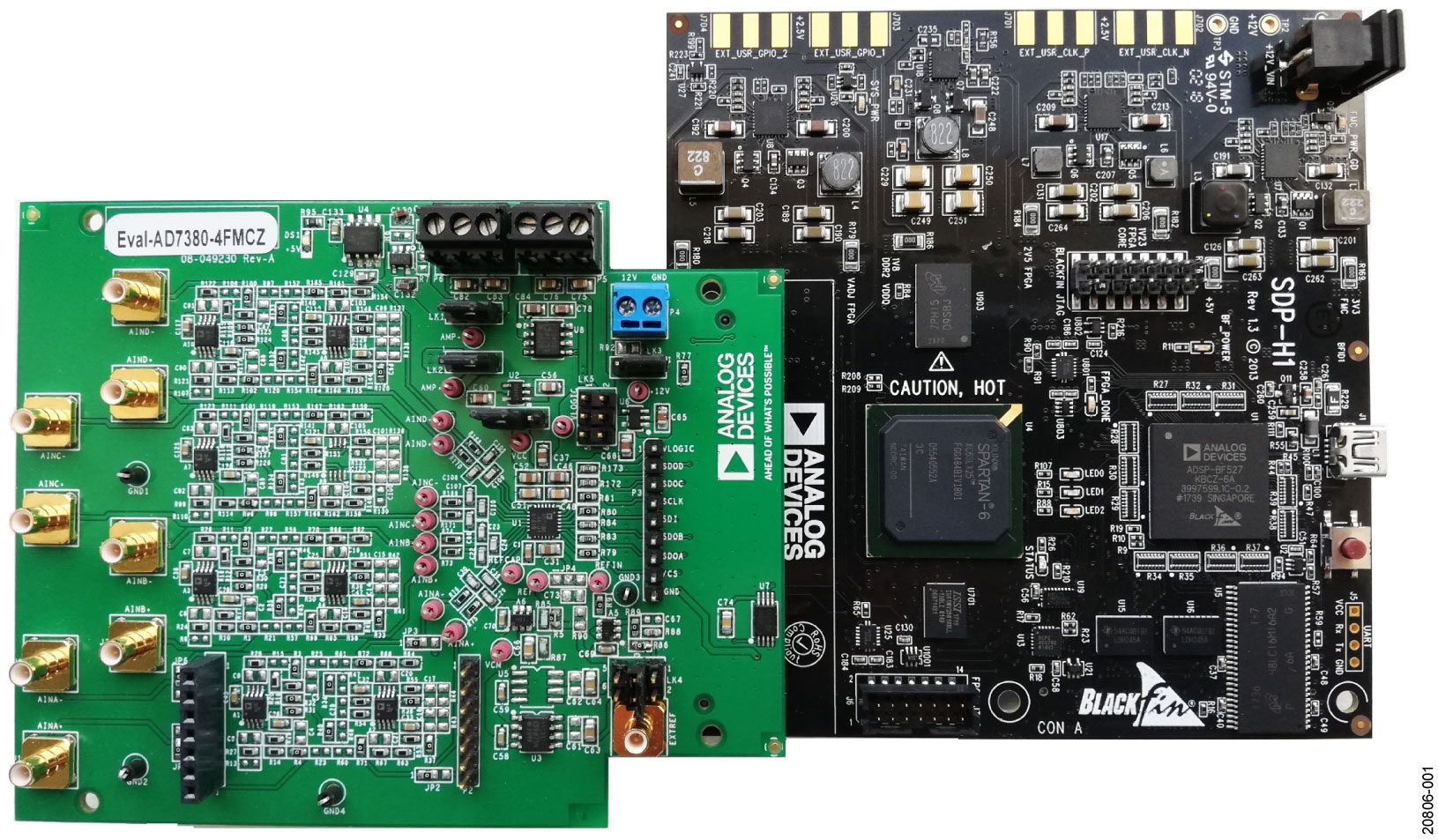
Figure 1 Figure 1. EVAL-AD7380-4FMCZ evaluation board (left) connected to SDP-H1 board (right).
Evaluation Board Quick Start Guide
The EVAL-AD7380-4FMCZ is powered by the SDP-H1 board by default. External power supplies can be applied. See Table 1 for a description of connectors required and Table 2 for the link configuration required. To evaluate the AD7380-4 with the EVAL-AD7380-4FMCZ, take the following steps:
Download and install the ACE software, which is available on the AD7380-4 product page. Installation details are found on the internal label of the EVAL-AD7380-4FMCZ box. Ensure that the SDP-H1 board is disconnected from the USB port of the PC when installing the ACE software. The PC may need to be restarted after the installation.
Ensure that the link options are configured as detailed in Table 2.
Connect the SDP-H1 board to the EVAL-AD7380-4FMCZ via the 160-way connector, as shown in Table 2.
Connect the SDP-H1 board to the PC via the USB cable.
If using Windows® XP, search for the SDP-H1 drivers. Choose to automatically search for the drivers for the SDP-H1 board if prompted by the operating system.
Copy the ACE plugins file, Board.AD738x, and the Chip.AD738x file from the EVAL-AD7380-4FMCZ evaluation board page to the
C:\ProgramData\Analog Devices\ACE\Pluginsfolder.Connect a −2.5V external power supply on the AMP− of the P6 connector terminal.
Launch the ACE software from the ACE subfolder in the Analog Devices folder in the All Programs menu.
Connect an input signal to Channel A, Channel B, Channel C, or Channel D.
Evaluation Board Connection Diagram
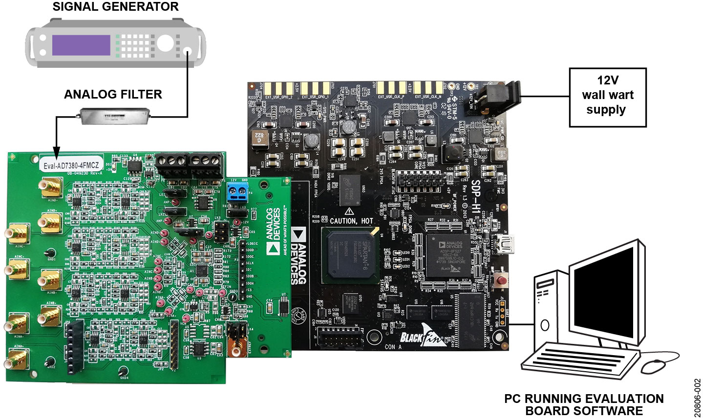
Figure 2 Figure 2. Typical setup of the EVAL-AD7380-4FMCZ and the SDP-H1 board.
Evaluation Board Hardware
Power Supplies
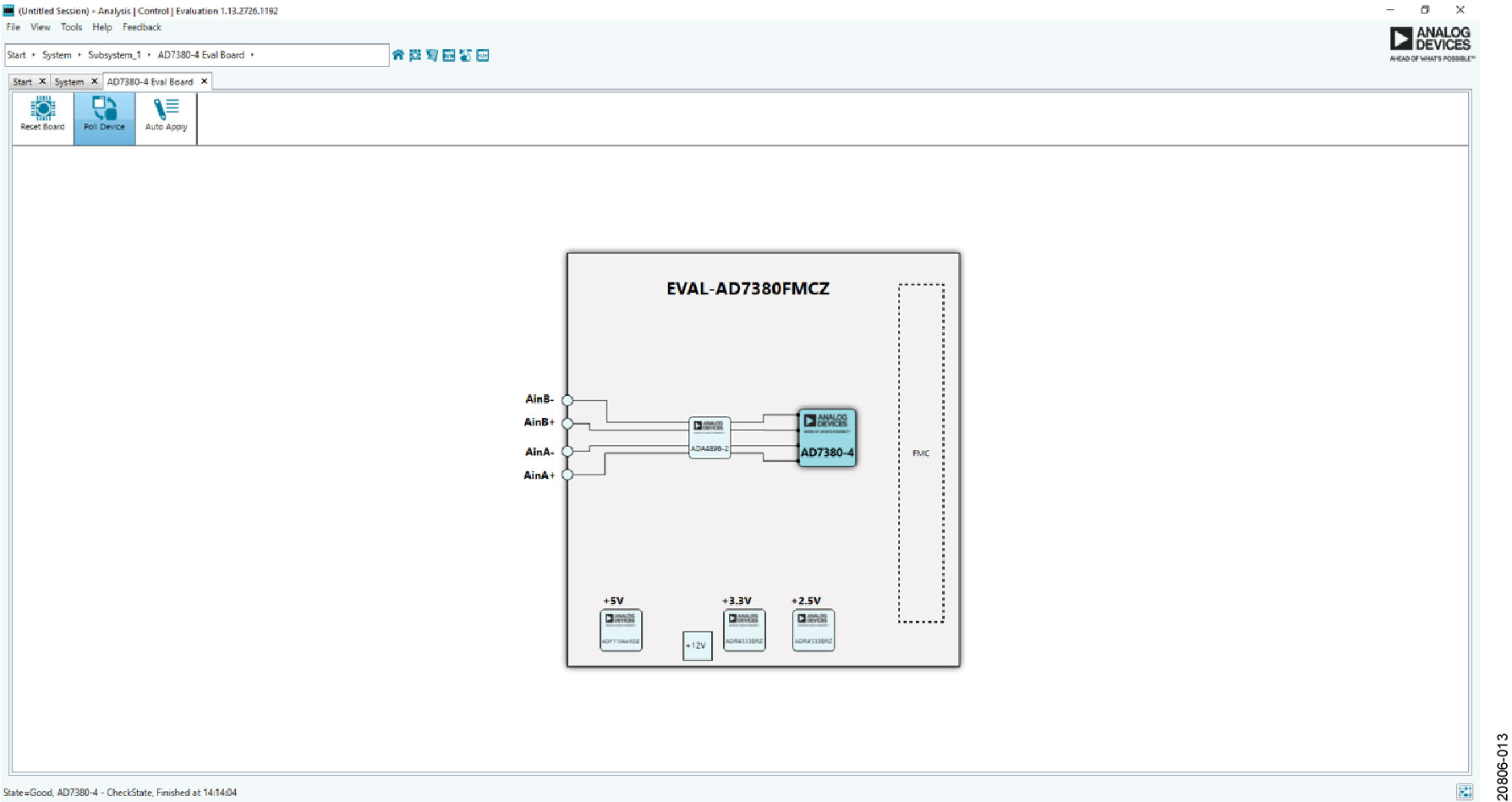
Ensure that all link positions are set according to the required operating mode before applying power and signals to the EVAL-AD7380-4FMCZ. See Table 2 for the complete list of link options. The EVAL-AD7380-4FMCZ is powered by the SDP-H1 board by default. External power supplies can also be applied to the board. See Table 1 for a description of the connectors used and Table 2 for the link configurations required. Figure 3 shows the functional block diagram of the EVAL-AD7380-4FMCZ with the onboard AD7380-4.
Table 1. Optional External Power Supplies
Power Supply |
Connector |
Voltage Range |
Description |
|---|---|---|---|
12V |
P4-1 |
12+/- 10% |
Mainboard power supply for all internal voltage regulators |
GND |
P4-2 |
0 |
Ground |
EXT_VCC |
P5-1 |
3.3+/- 5% |
ADC analog power supply |
GND |
P5-2 |
0 |
Ground |
EXT_VLOGIC |
P5-3 |
2.3+/- 5% |
Digital serial peripheral input (SPI) power supply |
EXT_AMP_PWR+ |
P6-1 |
5 +/- 5% |
Amplifier positive power supply |
EXT_GND |
P6-2 |
0 |
Ground |
EXT_AMP_PWR- |
P6-3 |
-2.5 +/- 5% |
Amplifier negative power supply |
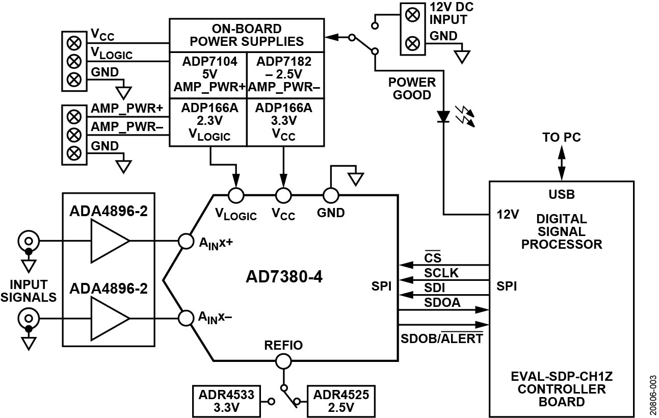
Figure 3 Figure 3. EVAL-AD7380-4FMCZ functional block diagram.
Link Configuration Options
Multiple link options must be set properly to select the appropriate operating setup before using the EVAL-AD7380-4FMCZ. The functions of these options are detailed in Table 2.
Setup Conditions
Ensure that all link positions are set as required by the selected operating mode before applying power and signals to the EVAL-AD7380-4FMCZ. Table 2 shows the default positions of the links when the EVAL-AD7380-4FMCZ is packaged.
Table 2. Link Options for EVAL-AD7380-4FMCZ
Link Name |
Function |
Default Position |
Description |
|---|---|---|---|
LK1 |
Internal or external selection for the negative supply of the amplifier |
1 |
Use the internal −2.5 V from the onboard ADP7182 for the negative supply of the amplifier via the ADP5600. |
LK2 |
Internal or external selection for the positive supply of the amplifier |
1 |
Use the internal 5 V from the onboard ADP7104 for the positive supply of the amplifier. |
LK3 |
Internal or external selection for the 12 V supply |
1 |
Use the 12 V power supply from the SDP-H1 board. Change to Position 3 to use an external supply. |
LK4 |
Selection for the external voltage reference (VREF) of the ADC |
3-4 |
Use the internal 3.3 V from the ADR4533 for VREF. Change to Position 5 connected to Position 6 (Position 5-6) to use the internal 2.5 V from the ADR4525. |
LK5 |
Selection for the logic voltage (VLOGIC) of the ADC |
3-4 |
Change to Position 1-2 (link shorted on Pin 1 and Pin 2) to use the external source. Change to Position 3-4 (link shorted on Pin 3 and Pin 4) to use the onboard ADP166. Change to Position 5-6 (link shorted on Pin 5 and Pin 6) to use VLOGIC from the EVAL-SDP-CH1Z. |
JP1, JP2 |
Amplifier selection for AINA− |
1(SMD resistor) |
Use the onboard ADA4896-2 amplifier for signal conditioning. Change to Position 3 to use an external amplifier mezzanine card (AMC) instead of the onboard ADC driver. |
JP3, JP6 |
Amplifier selection for AINA+ |
1(SMD resistor) |
Use the onboard ADA4896-2 amplifier for signal conditioning. Change to Position 3 to use an external amplifier mezzanine card (AMC) instead of the onboard ADC driver. |
JP4 |
Selection for the VREF of the ADC |
3(SMD resistor) |
The REFIO pin is driven with the on-board reference. |
Evaluation Board Circuitry
Sockets and Connectors
The sockets and connectors on the EVAL-AD7380-4FMCZ are described in Table 3. The default interface to the EVAL-AD7380-4FMCZ is via the P7 connector, which connects the EVAL-AD7380-4FMCZ to the SDP-H1 board. When using the EVAL-AD7380-4FMCZ in standalone mode, communication is achieved via the P3 header pins.
Test Points
There are several test points and single-in-line (SIL) headers on the EVAL-AD7380-4FMCZ. These test points and headers provide access to the evaluation board signals to allow probing, evaluation and debugging.
Table 3. On-Board Sockets and Connectors
Connector |
Function |
|---|---|
J1 |
Analog Input for Channel A |
J2 |
Analog Input for Channel A |
J3 |
Analog Input for Channel B |
J4 |
Analog Input for Channel B |
J5 |
Analog Input for Channel C |
J6 |
Analog Input for Channel C |
J7 |
Analog Input for Channel D |
J8 |
Analog Input for Channel D |
P1 |
AMC Input |
P2 |
AMC Output |
P3 |
Digital SPI signals |
P4 |
Main board power supply (12 V) for all internal voltage regulators |
P5 |
ADC power supply and digital SPI power supply |
P6 |
Amplifier power supply |
P7 |
Field-programmable gate array (FPGA), mezzanine card (FMC) to low pin count (LPC), SDP connector |
EXT_REF |
External voltage reference |
Evaluation Board Software
Software Installation Procedure
Download the ACE software from the AD7380-4 product page and install the ACE software on the PC before using the EVAL-AD7380-4FMCZ. The installation process consists of the ACE software installation and the SDP-H1 driver installation. To ensure that the evaluation system is recognized when it is connected to the PC, install the ACE software and SDP-H1 driver before connecting the EVAL-AD7380-4FMCZ and the SDP-H1 board to the USB port of the PC. Note that all functionality is the same for the AD7389-4 and AD7381-4 with the chip view specific to the AD7389-4 or AD7381-4.
Installing the ACE Software
To install the ACE software, take the following steps:
Download the ACE software to a Windows-based PC.
Double click the ACEInstall.exe file to begin the installation. By default, the software is saved to the following location: C:\Program Files (x86)\Analog Devices\ACE.
A window appears asking for permission to allow the program to make changes to the PC. Click Yes to begin the installation process.
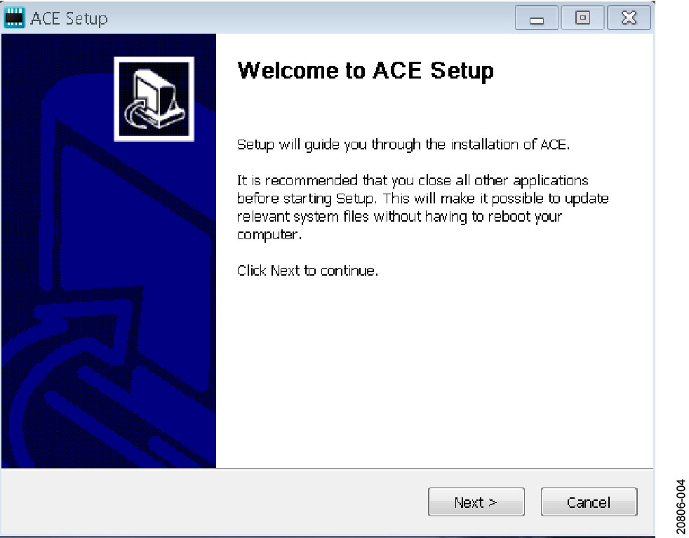
Click Next > to continue the installation, as shown in Figure 4.
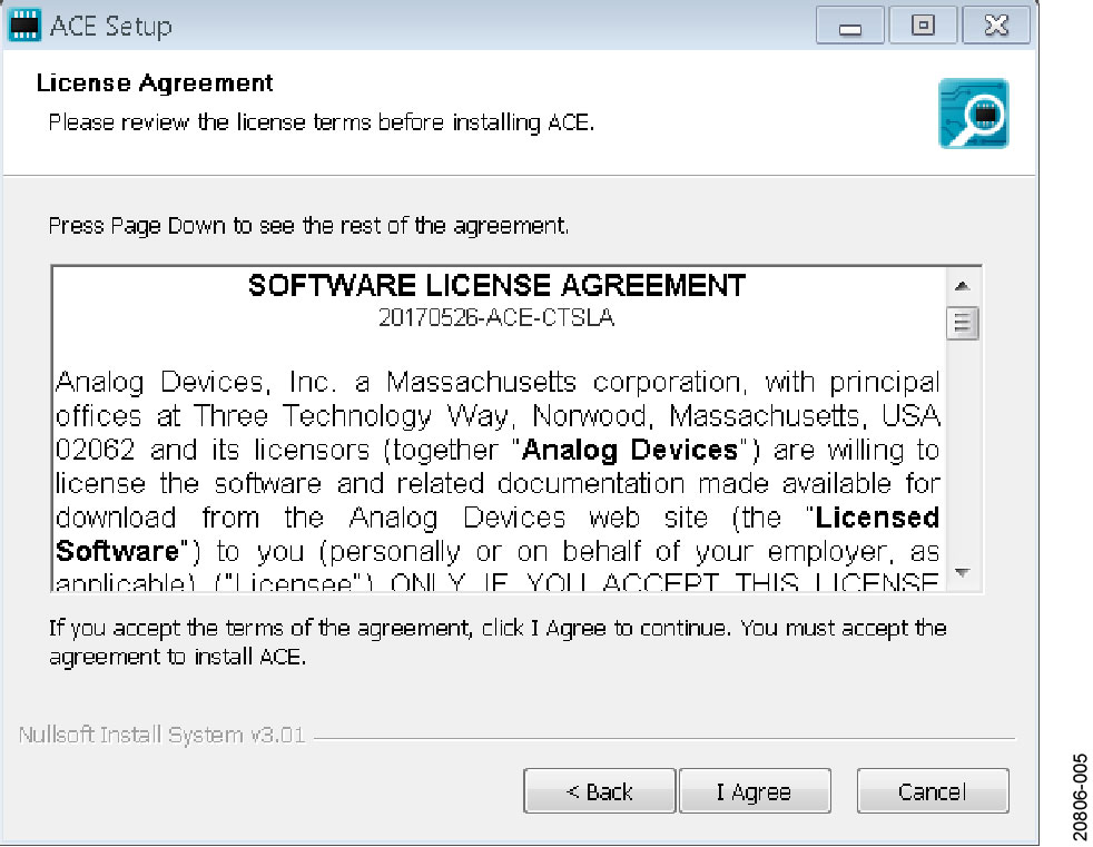
Read the software license agreement and click I Agree (see Figure 5).
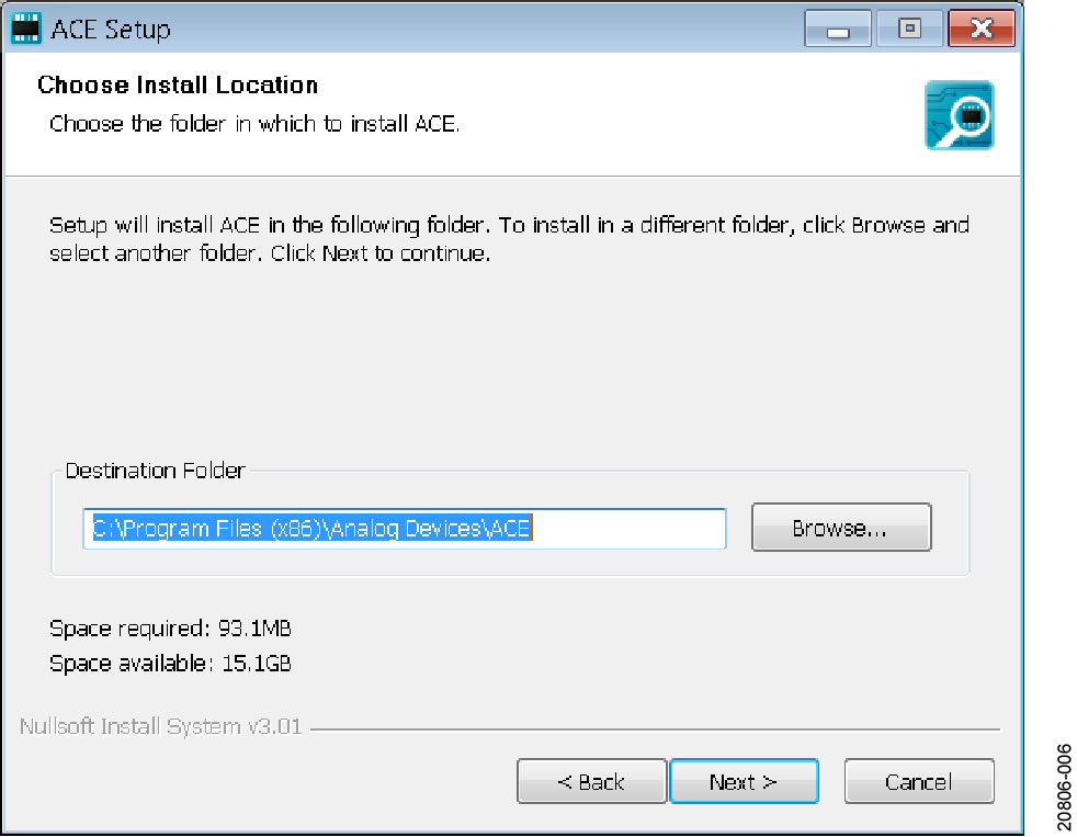
Choose an installation location and click Next > (see Figure 6).
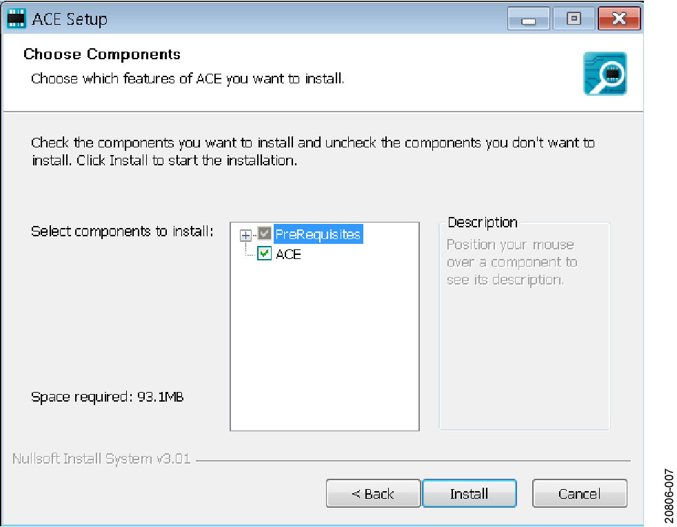
Select the PreRequisites checkbox to include the installation of the SDP-H1 driver and click Install (see Figure 7).
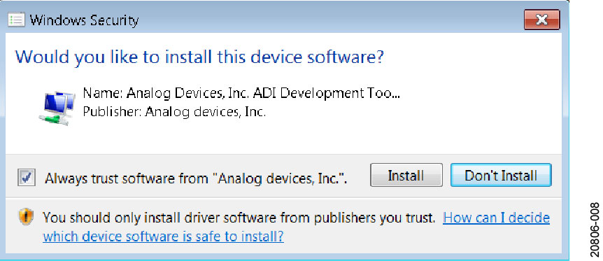
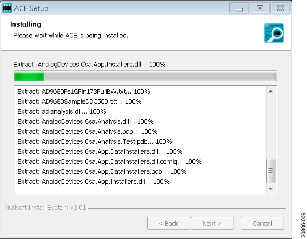
The Windows Security window appears. Click Install (see Figure 8). The installation is in progress. No action is required (see Figure 9).
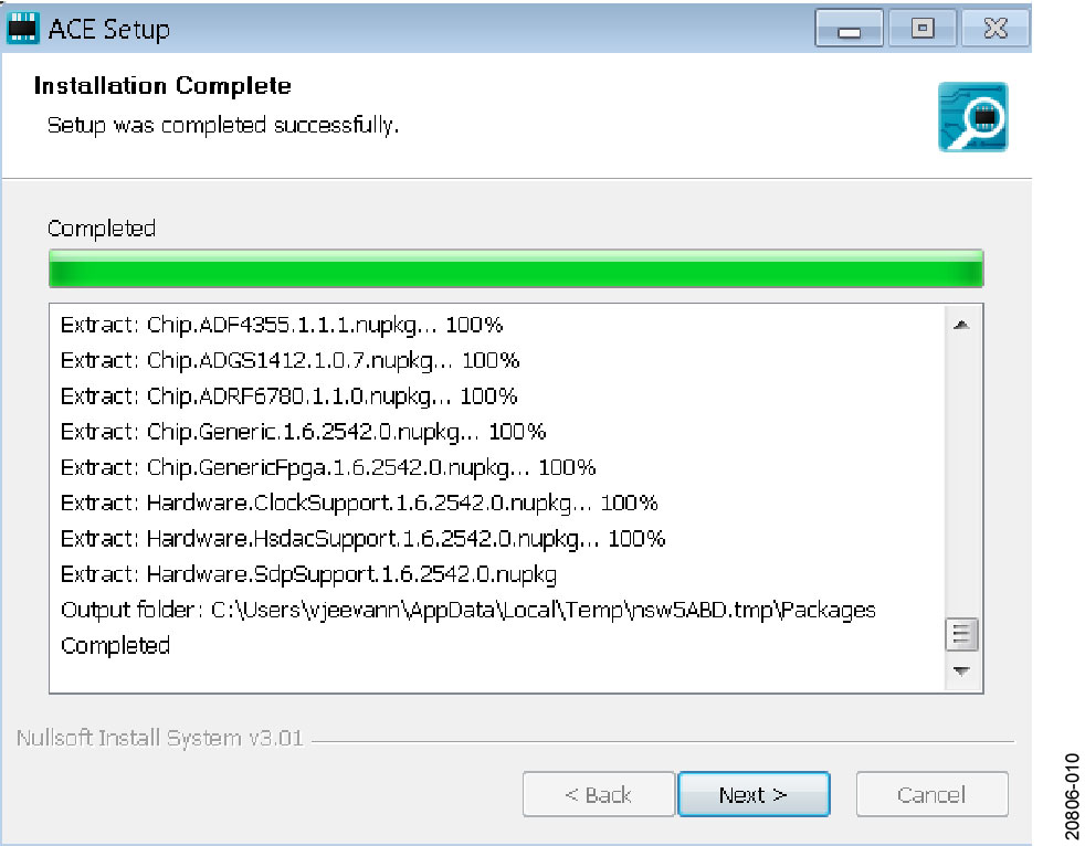
When the installation is complete (see Figure 10), click Next > and then click Finish to complete.
Evaluation Board Setup Procedures
Figure 2 shows a diagram of the connections between the EVAL-AD7380-4FMCZ and the SDP-H1 board. To ensure that the evaluation system is recognized when it is connected to the PC, install the ACE software and SDP-H1 driver before connecting the EVAL-AD7380-4FMCZ and the SDP-H1 board to the USB port of the PC. When the ACE software installation is complete, set up the EVAL-AD7380-4FMCZ and the SDP-H1 board as described in the following sections.
Connecting the EVAL-AD7380-4FMCZ and the SDP-H1 Board to the PC
To connect the EVAL-AD7380-4FMCZ and the SDP-H1 board to the PC, take the following steps:
Ensure that all configuration links are in the appropriate positions, as detailed in Table 2.
Connect the EVAL-AD7380-4FMCZ securely to the P7 connector on the SDP-H1 board. The EVAL-AD7380-4FMCZ does not require an external power supply adapter.
Connect the SDP-H1 board to the PC via the USB cable enclosed in the SDP-H1 kit.
Connect a −2.5 V supply to the AMP− pin of the P6 connector terminal.
Verifying Board Connection
To verify the board connection, take the following steps:
When the SDP-H1 board is plugged into the PC, allow the Found New Hardware Wizard to run. If using Windows XP, search for the SDP-H1 drivers. If prompted by the operating system, choose to automatically search for the drivers for the SDP-H1 board.
A window may appear asking for permission to allow the program to make changes to the computer. In this case, click Yes. The Computer Management window opens.
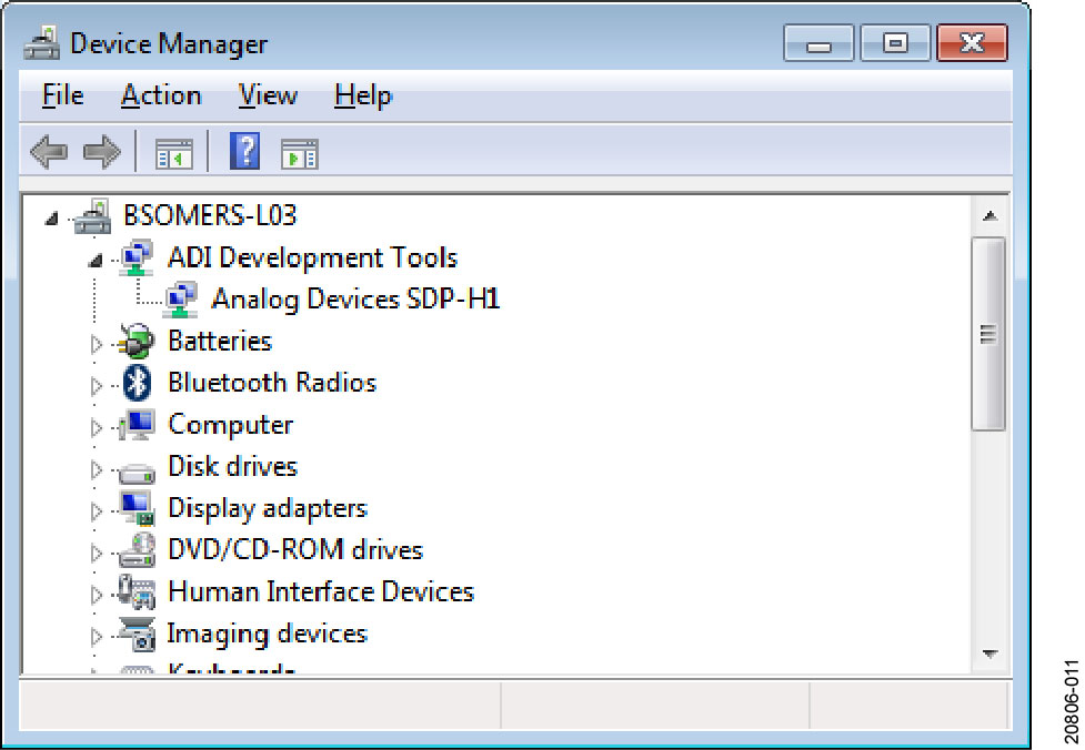
Under System Tools, click Device Manager and use the Device Manager window to ensure that the SDP-H1 board is connected to the PC properly. If the SDP-H1 driver software is installed and the board is connected to the PC properly, Analog Devices SDP-H1 appears under ADI Development Tools in the Device Manager window, as shown in Figure 11.
Disconnecting the EVAL-AD7380-4FMCZ
Always remove power from the SDP-H1 board and the EVAL-AD7380-4FMCZ or click the reset tact switch located alongside the USB port before disconnecting the EVAL-AD7380-4FMCZ from the SDP-H1 board.
Using the ACE Software for Testing
Launching ACE Software
When the EVAL-AD7380-4FMCZ and SDP-H1 boards are properly connected to the PC, launch the ACE software. To launch the ACE software, take the following steps (note that all functionality is the same for the AD7389-4 and the AD7381-4 with the chip view specific to the AD7389-4 or the AD7381-4):
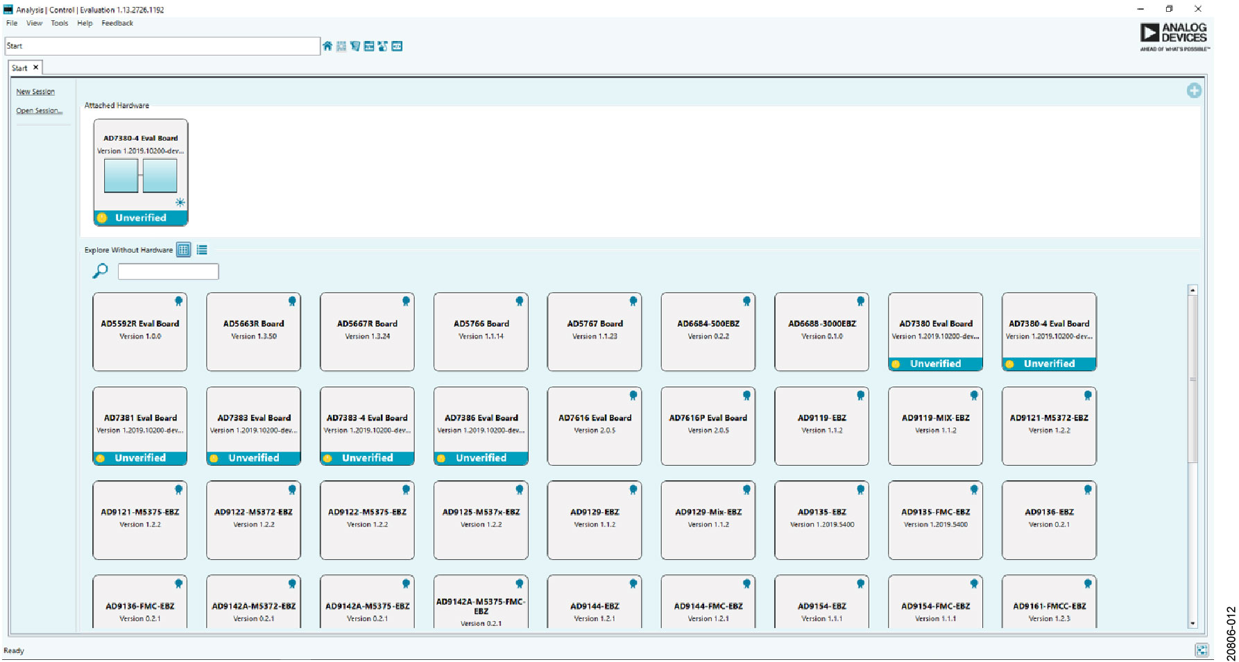
From the Start menu, select All Programs > Analog Devices > ACE > ACE.exe to open the main software window, as shown in Figure 12.
The AD7380-4 Eval Board icon appears in the Attached Hardware section. If the EVAL-AD7380-4FMCZ is not connected to the USB port via the SDP-H1 board when the software is launched, the AD7380-4 Eval Board icon does not appear in the Attached Hardware section. In this case, connect the EVAL-AD7380-4FMCZ and SDP-H1 board to the USB port of the PC, wait a few seconds, and then continue following these instructions.
Double click the AD7380-4 Eval Board icon to open the window shown in Figure 13.
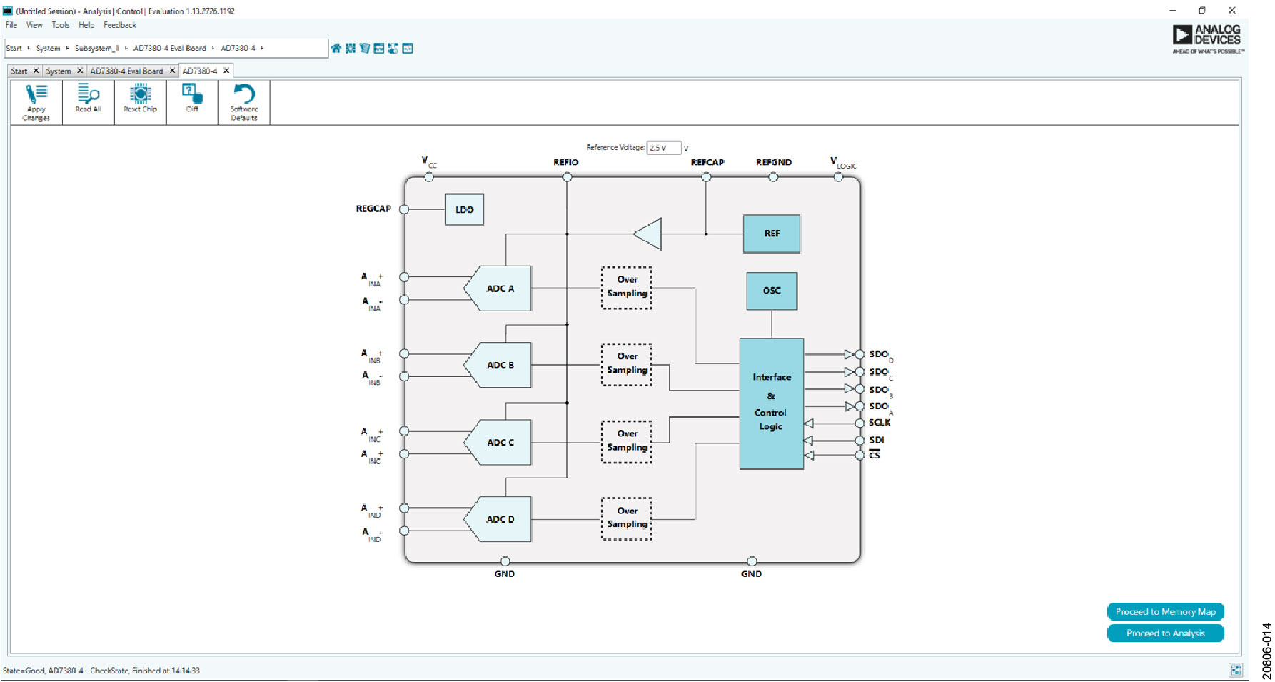
Double click the AD7380-4 chip icon to open the window shown in Figure 14.
Click Software Defaults and then click Apply Changes.
Chip View
When the software installation procedures and the evaluation board setup procedures are complete, set up the system for data capture by taking the following steps:
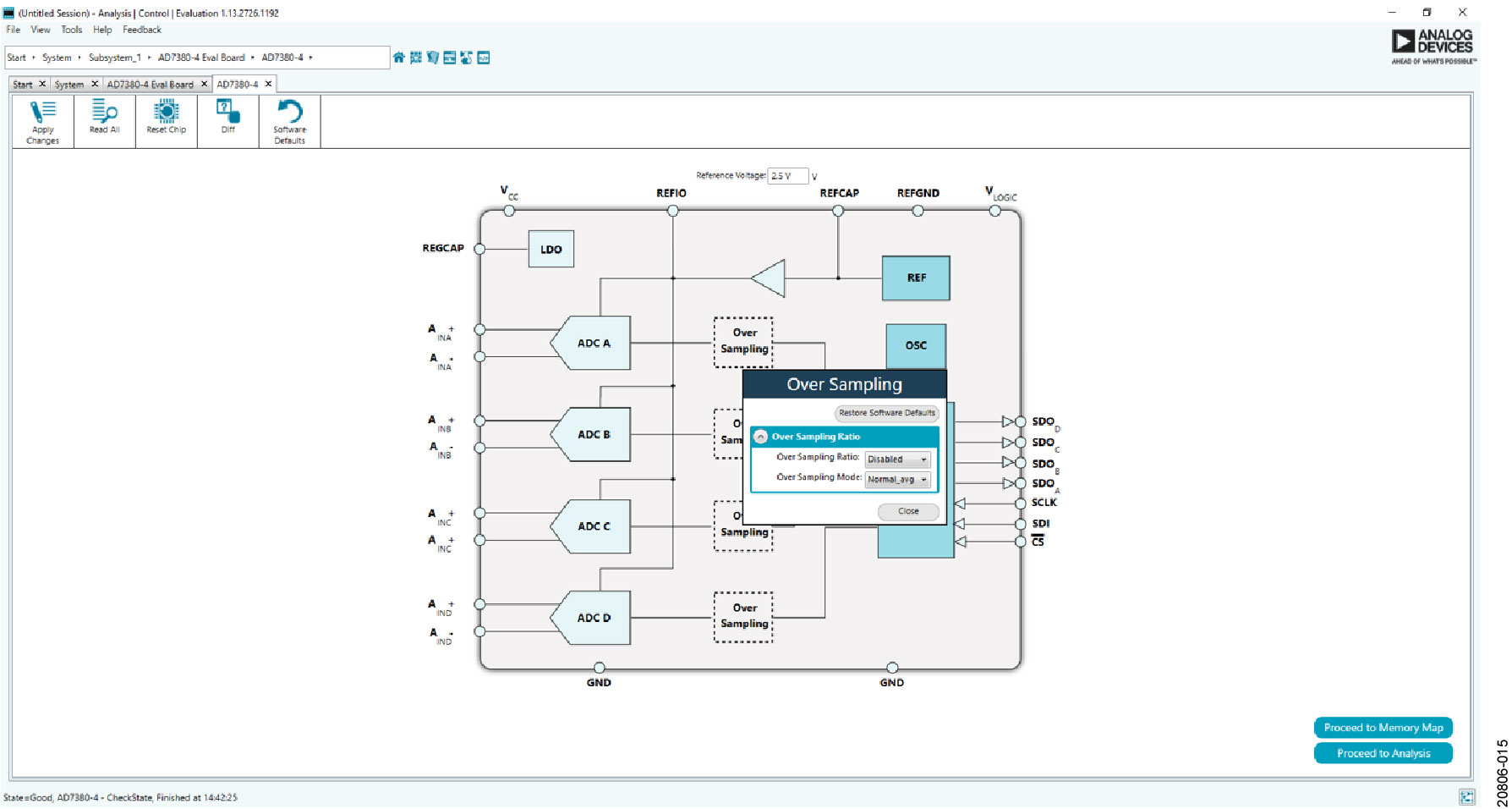
Block icons that are dark blue are programmable blocks. Click a dark blue block icon to open a configurable pop-up window that allows customization for data capture, as shown in the oversampling block in Figure 15.
Enter the reference voltage value in the Reference Voltage box at the top of the window when External Reference is selected. The default value for the external reference is set to 3.3 V.
See the Software Installation Procedures section and the Evaluation Board Setup Procedures section for additional information.
Memory Map Window Features
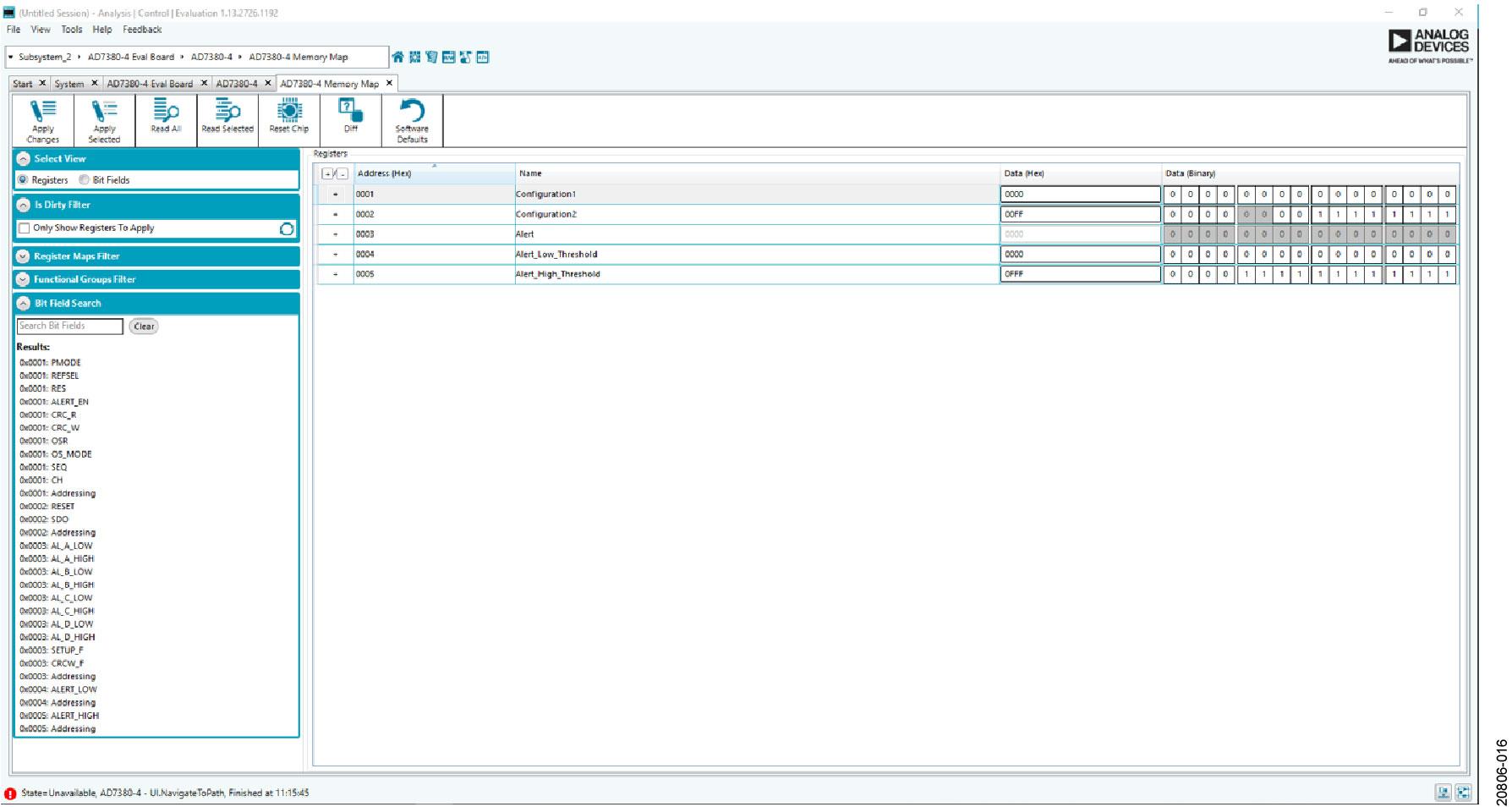
Click Proceed to Memory Map in the bottom right corner of the chip view (see Figure 14) to open the window shown in Figure 16. The memory map shows all AD7380-4 registers.
Apply Changes
The registers are in the default values at power up. To change the register values, click the + Icon next to the Address (Hex) column, then select the boxes that correspond to the configuration being edited. The values in the boxes toggle between 1 and 0. To apply the values changed to all registers, click Apply Changes to write to the registers.
Apply Selected
In some cases, the values of every register have changed, but the user may want to only implement changes on a selected register. To select a specific register, click the register name and then click Apply Selected to write a new value on a selected register to the AD7380-4.
Read All
Click Read All to read the values of all AD7380-4 registers.
Read Selected
To select a read, highlight the desired register to be read. Click Read Selected to read the selected AD7380-4 register(s).
Reset Chip
Click Reset Chip to allow the software to reset the AD7380-4.
Diff
Click Diff to check for differences in register values between the ACE software and the AD7380-4.
Software Defaults
To revert all register values back to the default values, click Software Defaults and then click Apply Changes to write to the AD7380-4.
Analysis View
Click Proceed to Analysis in the bottom right corner of the chip view window (see Figure 14) to open the analysis view window shown in Figure 17. The analysis view contains the Waveform tab, Histogram tab, and FFT tab.
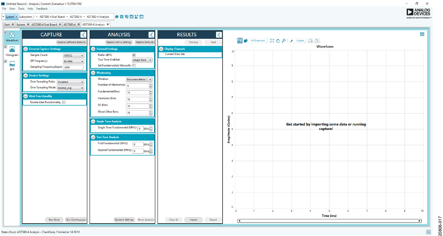
Waveform Tab
The Waveform tab displays data in the form of time vs. discrete data values with the results, as shown in Figure 18. The Capture pane contains the capture settings, which reflect onto the registers automatically before data capture.
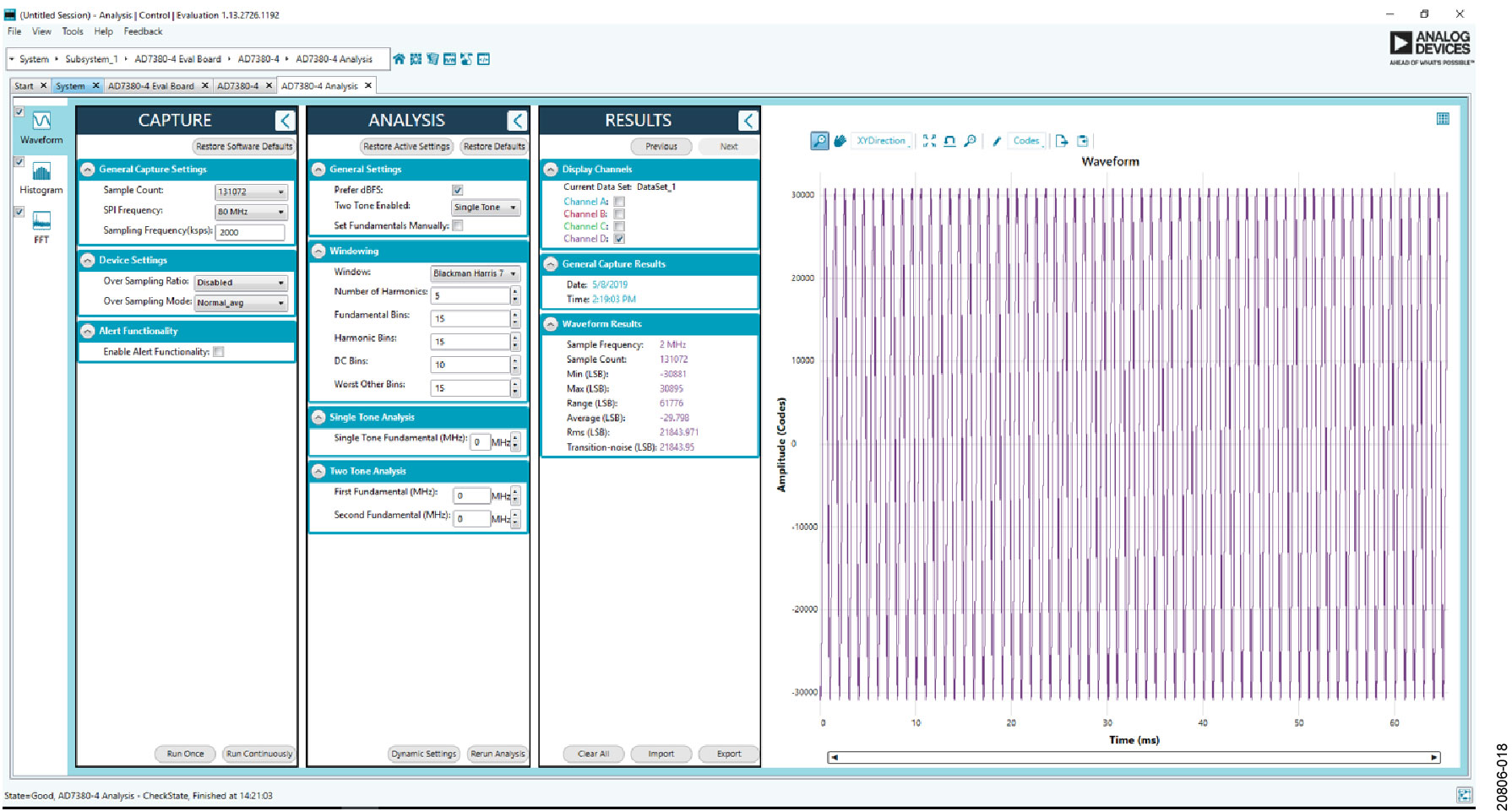
Capture Pane
The Sample Count dropdown list in the General Capture Settings section allows the user to select the number of samples per channel per capture.
The SPI Frequency dropdown list in the General Capture Settings section allows the user to select the SPI clock frequency used to transfer data between the FPGA device integrated onto the SDP-H1 board and the AD7380-4 during device register reads and writes and during data capture. This frequency must be set higher than the set throughput rate.
The user can enter the input sample frequency in kSPS in the Sampling Frequency (ksps) box in the General Capture Settings section. Refer to the AD7380-4 datasheet to determine the maximum sampling frequency for the selected mode. The Over Sampling Ratio dropdown list in the Device Settings section, when enabled, can be set from 2 to 32 and provides an improved signal to noise ratio (SNR) performance. Refer to the AD7380-4 datasheet to determine the maximum oversampling ratio for the selected oversampling mode.
The Over Sampling Mode dropdown list in the Device Settings section allows the user to select the oversampling mode. This setting is only applicable when over-sampling is enabled.
When a value is chosen from the Over Sampling Ratio dropdown list, select 18-Bit Resolution from the pop-up box that opens to place the device in 18-bit resolution mode. The resolution boost is used in conjunction with the oversampling rate to provide two extra bits of resolution.
Click Run Once in the Device Settings section to start a data capture of the samples at the sample rate specified in the Sample Count dropdown list. These samples are stored on the FPGA device and are only transferred to the PC when the sample frame is complete.
Click Run Continuously in the Device Settings section to start a data capture that gathers samples continuously with one batch of data at a time.
Result Pane (Waveform Tab)
The Display Channels section allows the user to select which channels to capture. The data for a specific channel is only shown if that channel is selected before the capture. The Waveform Results section displays amplitude, sample frequency, and noise analysis data for the selected channels. Click Export in the Results pane to export captured data. The waveform, histogram, and fast Fourier transform (FFT) data is stored in .xml files along with the values of parameters at capture.
Waveform Graph
The data waveform graph shows each successive sample of the ADC output. The user can zoom in on and pan across the waveform graph using the embedded waveform tools. The channels to display can be selected in the Display Channels section of the Results pane. Click the display units dropdown list (shown with the Codes option selected in Figure 18) to select whether the data graph displays in units of Hex, volts, or codes. The axis controls are dynamic. When selecting either y-scale dynamic or x-scale dynamic, the corresponding axis width automatically adjusts to show the entire range of the ADC results after each batch of samples.
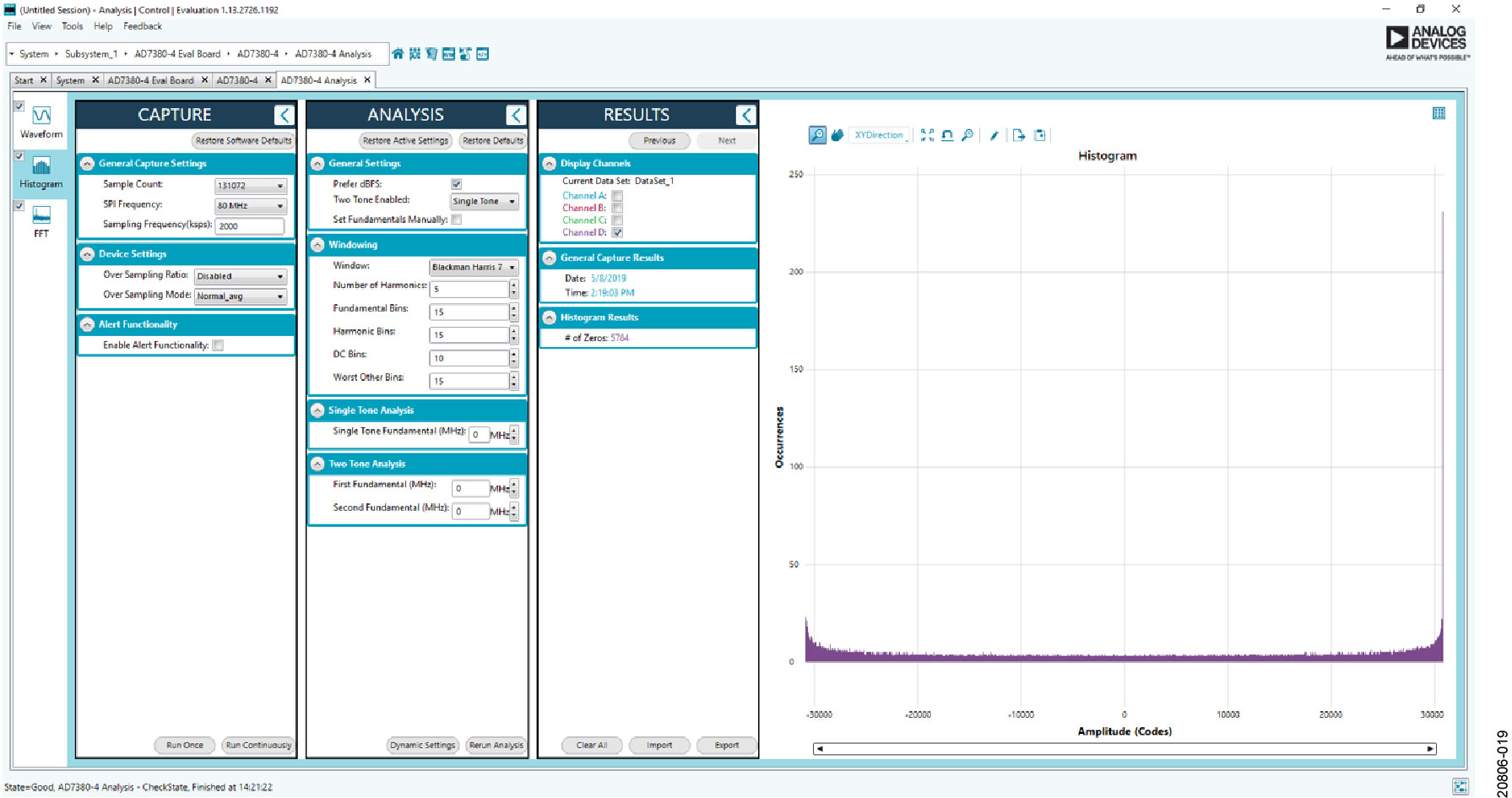
Histogram Tab
The Histogram tab contains the histogram graph and the Results pane, as shown in Figure 19. The Results pane displays the information related to the ADC performance. The histogram graph displays the number of hits per code within the sampled data. This graph is useful for dc analysis and indicates the noise performance of the device.
FFT Tab
The FFT tab displays FFT information for the last batch of samples gathered, as shown in Figure 20.
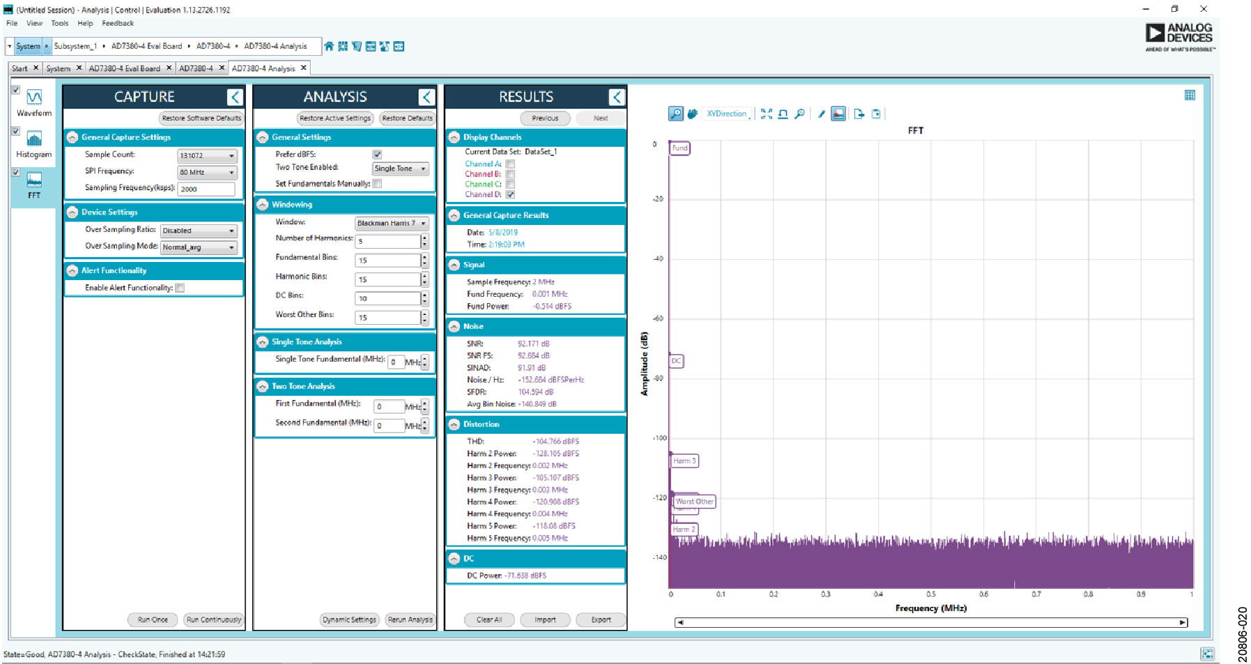
Analysis Pane
The General Settings section allows the user to set up the preferred configuration of the FFT analysis. This configuration sets how many tones are analyzed and if the fundamental is set manually. The Windowing section allows the user to set up the preferred windowing type to use in the FFT analysis and the number of harmonic bins and fundamental bins that must be included in the analysis. The Single Tone Analysis and the Two Tone Analysis sections sets up the fundamental frequencies included in the FFT analysis. When one frequency is analyzed, use the Single Tone Analysis section. When two frequencies are analyzed, use the Two Tone Analysis section.
Results Pane
The Signal section displays the sample frequency, fundamental frequency, and fundamental power. The Noise section displays the SNR and other noise performance results. The Distortion section displays the harmonic content of the sampled signal and dc power when viewing the FFT analysis.
Exiting the Software
To exit the software, click File and then click Exit.
Evaluation Board Design Files
Board schematic, layout and BOM files: eval-ad7380-4fmcz_design_files.zip