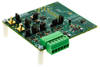
EVAL-AD35XXR
16-Bit / 12-Bit, Dual-Channel, 33 MSPS Ultrafast Current Output DAC Evaluation Board.
Overview
The EVAL-AD3552RFMCxZ are the evaluation boards for the AD3552R, a low drift, dual-channel, ultra-fast, 16-bit accuracy, current output digital-to-analog converter (DAC). The board is also compatible with the AD3542R, a 12-bit variant of the same family.
Both board variants share the same FMC connector pinout. The FMC1Z is optimized for high-speed dynamic performance. The FMC2Z is optimized for DC precision, using a lower bandwidth transimpedance amplifier.
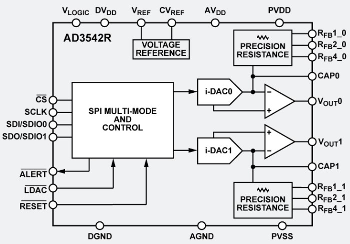
The AD3552R operates with a fixed 2.5 V internal reference and incorporates three drift-compensating feedback resistors for the required external transimpedance amplifier (TIA). Offset and gain scaling registers allow generation of multiple output voltage spans: 0 V to 2.5 V, 0 V to 5 V, 0 V to 10 V, −5 V to +5 V, and −10 V to +10 V. The device supports Fast Mode (16-bit) for maximum speed and Precision Mode (24-bit) for maximum accuracy, and can operate with Single, Dual, or Quad SPI interfaces up to 33 MSPS per channel.
The evaluation board interfaces with an FPGA carrier via an FMC LPC connector, using the ZedBoard (Zynq-7000 SoC) as the supported FPGA platform.
Features:
16-bit (AD3552R) or 12-bit (AD3542R) resolution
Dual-channel, simultaneous output
Up to 33 MSPS update rate per channel in Quad SPI Fast Mode
Configurable output ranges: 0 V to 2.5 V, 0 V to 5 V, 0 V to 10 V, ±5 V, ±10 V
Single, Dual, or Quad SPI digital interface
Fixed 2.5 V internal reference (or external reference via J3)
On-board ±12 V transimpedance amplifier power supply
Selectable TIA gain via link options (J-FB0, J-FB1)
External clock (J1) and trigger (J2) inputs for synchronization
Voltage outputs on SMB connectors J4 (CH0) and J5 (CH1)
Applications:
Waveform generation and arbitrary signal synthesis
Test and measurement instrumentation
Industrial control and automation
Precision power supply control
Recommendations
People who follow the flow that is outlined have a much better experience with things. However, like many things, documentation is never as complete as it should be. If you have any questions, feel free to ask on our EngineerZone, but before that, please make sure you read our documentation thoroughly.
To better understand the AD3552R, we recommend using the EVAL-AD3552RFMCxZ evaluation board together with the ZedBoard FPGA development kit.
Table of contents
Using the evaluation board/full stack reference design that we offer:
Prerequisites - what you need to get started
-
Using the ZedBoard
Linux Applications
Design with the AD3552R / AD3542R
Resources for designing a custom AD3552R-based platform:
For Linux software:
About the device driver:
For No-OS software:
HDL reference design which you must use in your FPGA.
Block diagram
The AD3552R HDL reference design on the ZedBoard uses the AXI AD35XXR IP core to interface the DAC via a Quad SPI bus. The AXI-DMAC streams sample data from DDR memory to the IP core, which serializes it and drives the AD3552R at up to 33 MSPS per channel.
ADI articles
Warning
All the products described on this page include ESD (electrostatic discharge) sensitive devices. Electrostatic charges as high as 4000V readily accumulate on the human body or test equipment and can discharge without detection. Although the boards feature ESD protection circuitry, permanent damage may occur on devices subjected to high-energy electrostatic discharges. Therefore, proper ESD precautions are recommended to avoid performance degradation or loss of functionality. This includes removing static charge on external equipment, cables, or antennas before connecting to the device.