EVAL-ADA4355EBZ
General Description
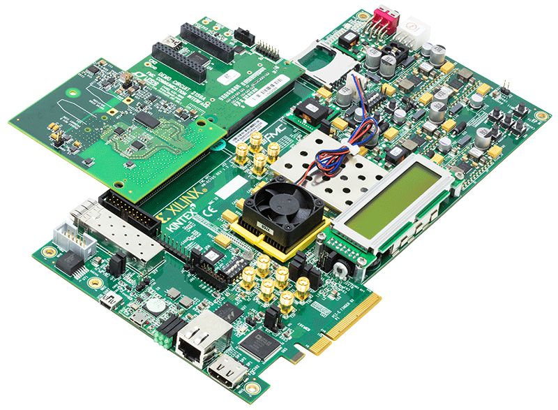
The ADA4355 evaluation system is used to evaluate the performance of the ADA4355 receive uModule. The system couples the Analog Devices ADA4355 evaluation board to a Xilinx KC705 FPGA evaluation platform. The KC705 provides ample memory, GPIOs and processing power to perform all control and data manipulation functions. All evaluation system control and data processing is accomplished via a MATLAB-based graphical user interface.
Getting Started
Installing the Software
Install the software before connecting the FMC communication board to the USB port of the PC.
Important
When the software is installed the default location will be
C:\Program Files\Analog Devices\ADA4355. If you do not have
write privileges at this location, choose another location where
you do have write privileges, typically under
C:\Users\<user_name>.
Start the Windows Operating System and download the software, ADA4355 Evaluation Software, provided in the Downloads section.
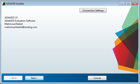
Launch the evaluation board software installation by clicking the ADA4355.exe file. The software installation window opens as shown in the figure below. To continue click Next.
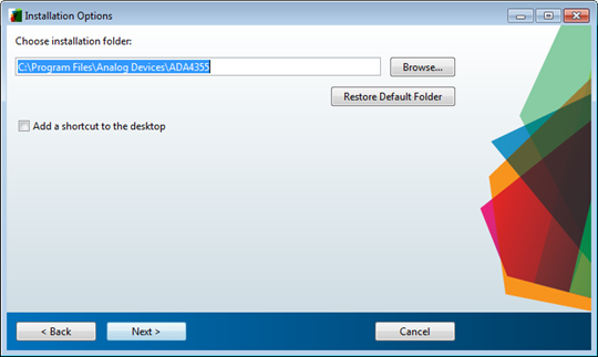
Choose the folder location for installation and click Next. If desired, a shortcut can be added to the PC desktop.
Important
The software must be installed in a location where you have write privileges.
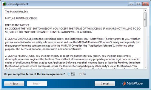
The evaluation software requires a MATLAB Runtime engine. If the MATLAB Runtime engine is already installed, this step is skipped. Choose the location for the installation of the Runtime engine and click Next.
Accept the MathWorks software license agreement and click Next. The Runtime engine download is about 700 MB. Ensure there is sufficient free hard drive space on the PC.
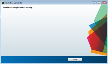
Click Finish to complete the installation.
Connect and power up the evaluation system as described in the Powering Up section.
Hardware
ADA4355 Evaluation System
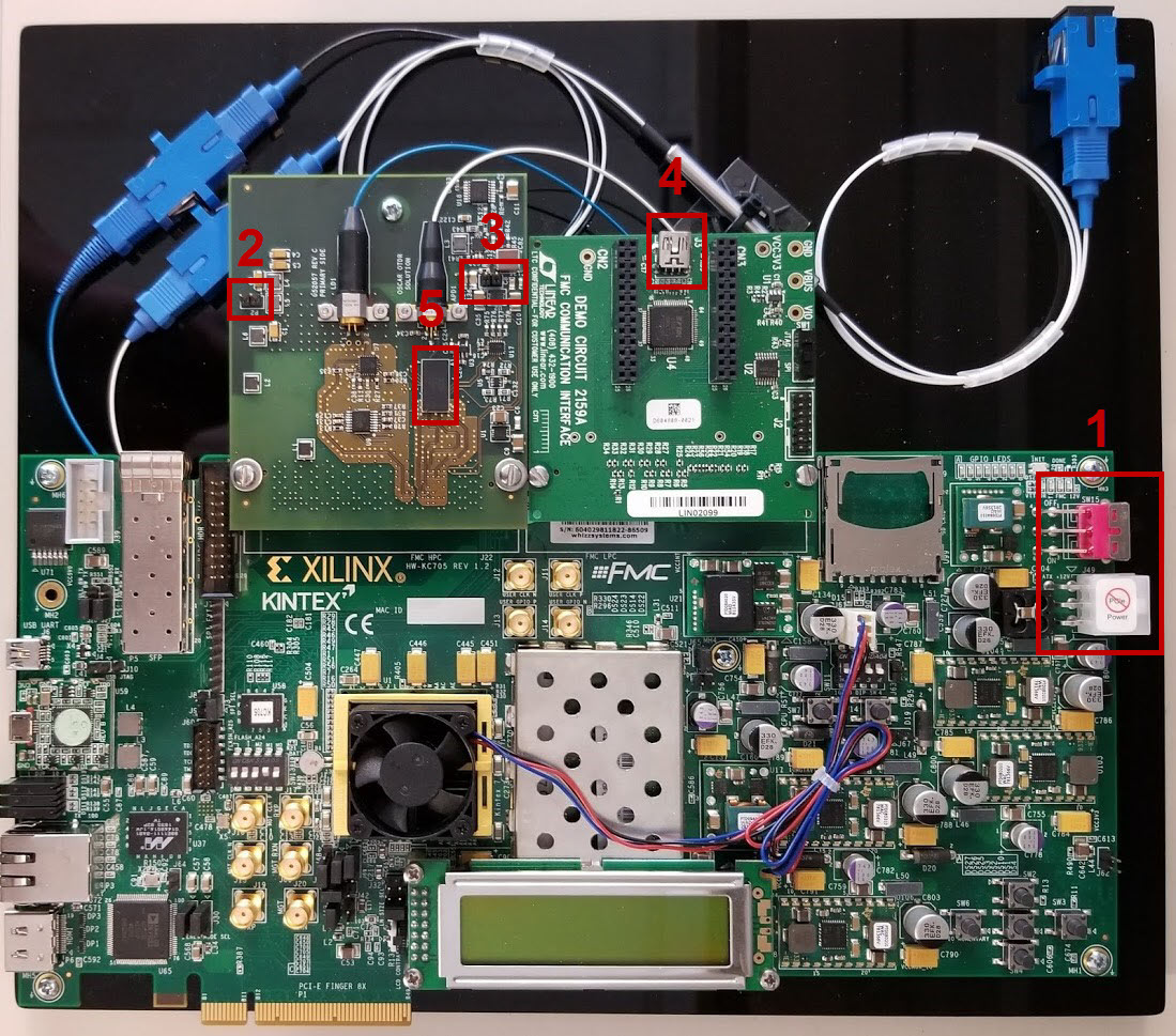
12 V FPGA board supply and on/off switch
5 V ADA4355 evaluation board supply (see figure below)
Optional external photo diode (APD) voltage supply connector (see APD bias figure below)
DC2159A communication interface board USB port
ADA4355 receive uModule
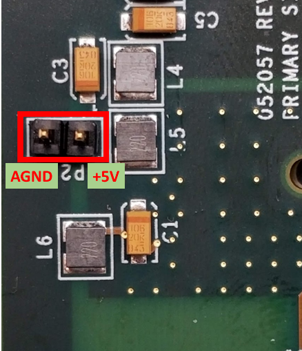
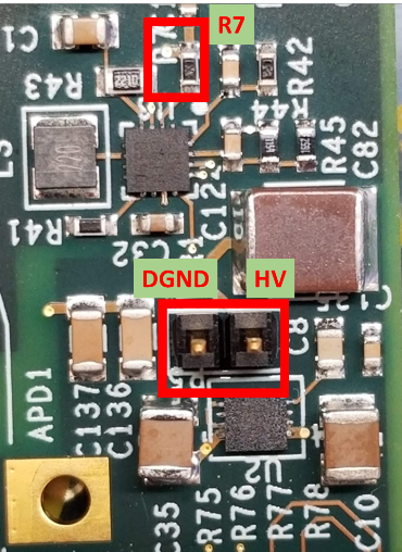
Figure 8 Optional high-voltage photo detector bias voltage connection detail (Header P5 and Resistor R7)
Powering Up
The ADA4355 evaluation system requires two power supplies: a 12 V supply for the FPGA board and a clean, well-regulated, 5 V supply (user to provide) for the ADA4355 board. Additionally, a high voltage supply is needed to reverse bias the photo detector. The evaluation system includes an on-board high-voltage bias generator that is fully controlled via the GUI. Alternatively, the user has the option to supply their own photo detector bias voltage through header P5.
All connection points are indicated in the evaluation system figure above. Detail for the 5 V supply connection is also shown in the 5 V connection figure, while detail for the optional, user-supplied, high-voltage reverse bias connection (HV) is shown in the bias voltage figure.
If supplying your own photo detector reverse bias voltage, the 10 Ohm resistor R7 (shown in the bias voltage figure) should be removed from the ADA4355 evaluation board prior to making any supply connections.
Evaluation system connection instructions are as follows:
Connect the 12 V supply to the FPGA board.
Connect the included USB cable from the PC to the USB port on the LTC communication interface board.
Connect the user-provided 5 V power supply to the ADA4355 evaluation board. See the 5 V connection figure for details.
If using the on-board bias generator (default), skip this step and leave header P5 unconnected. If providing your own photo detector reverse bias voltage, ensure that 10 Ohm resistor R7 has been removed and apply the desired reverse bias voltage at pin 1 (HV) of header P5.
Software Operation
Setup and Measurement Configuration
Start up the software by double clicking the desktop shortcut (if present), or navigate to the directory location chosen during installation, and under the application subfolder, run ADA4355.exe. You may also search in all programs for ADA4355.exe to launch the software.
Note
Due to initialization of the MATLAB runtime engine, initial start-up after reboot could take up to 2 minutes.
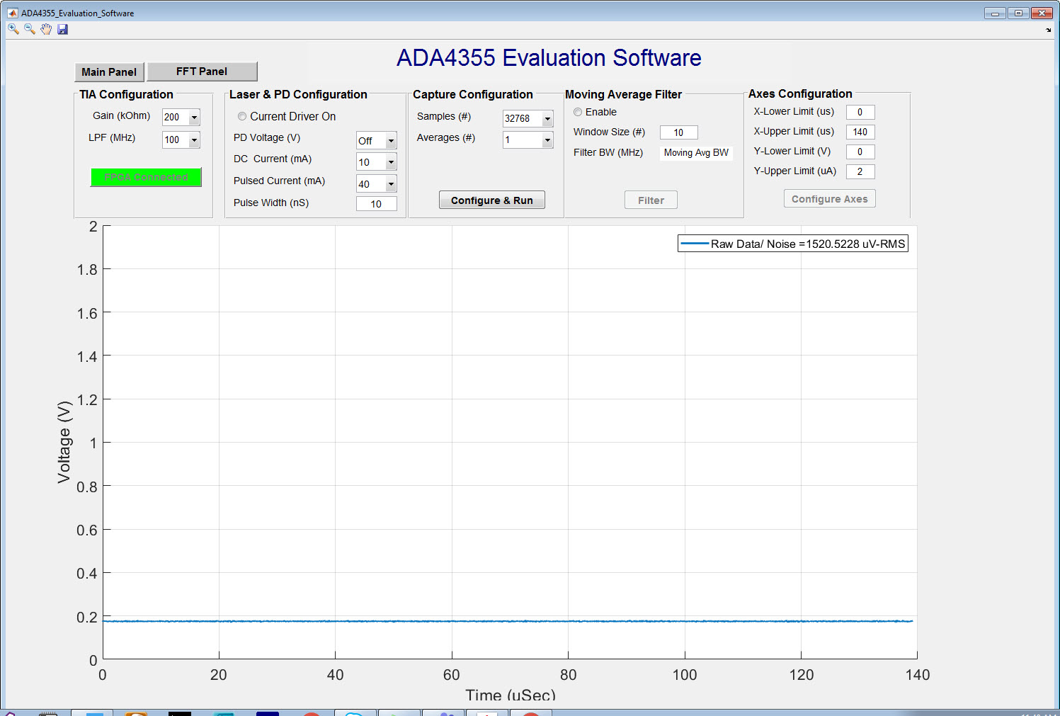
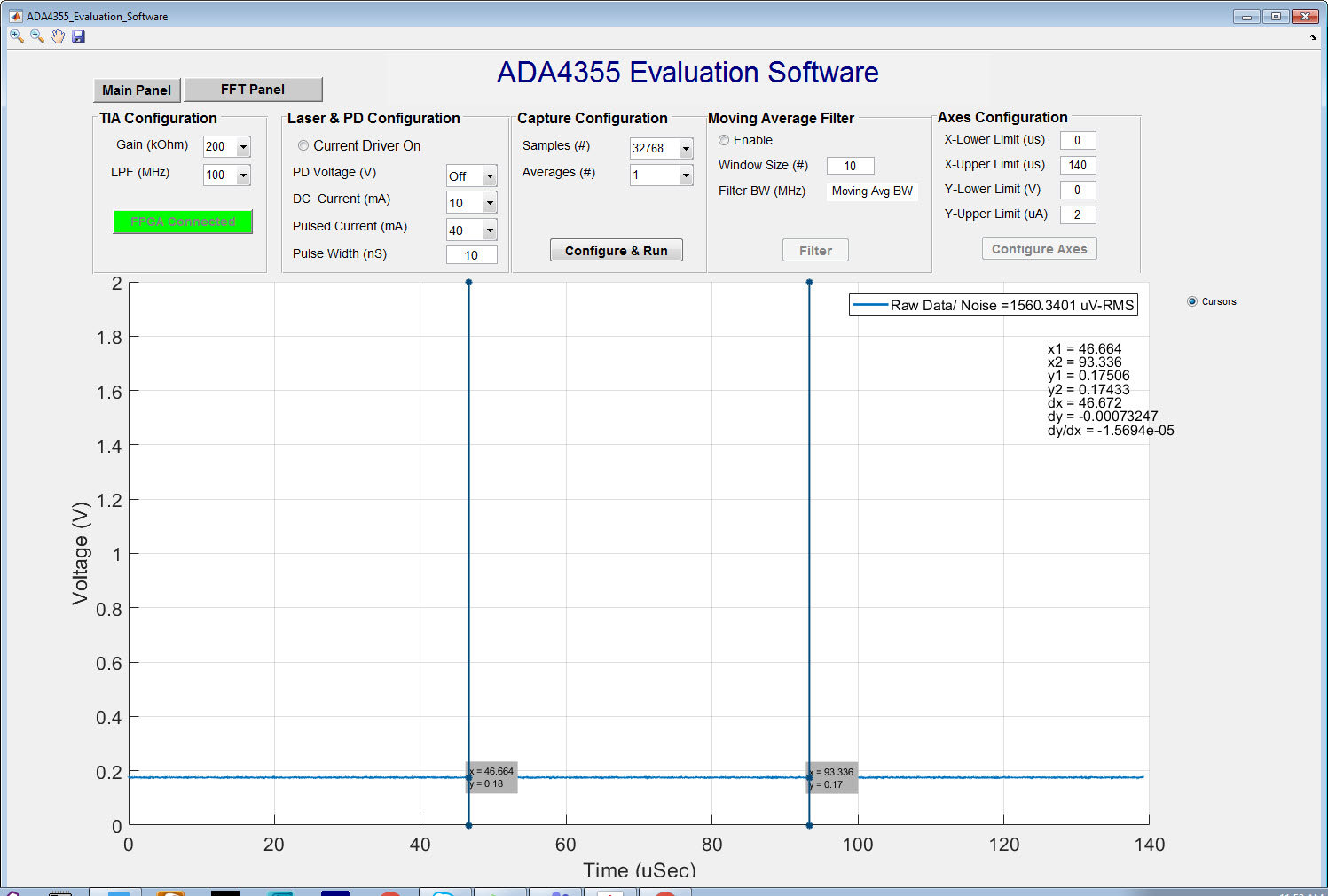
Once the software starts up, the main user panel is shown. Note the Connect to FPGA button is red indicating that the software is not yet connected to the evaluation system. Click the Connect to FPGA button to initiate connection to the system.
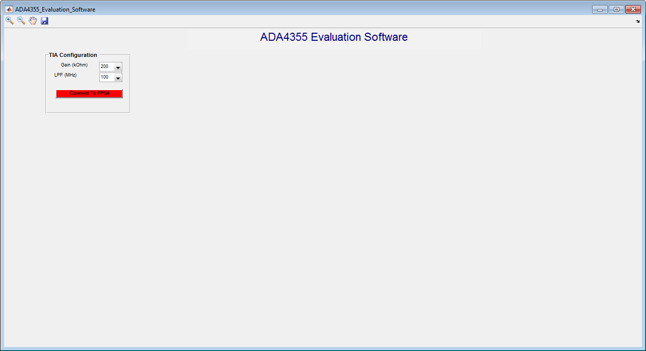
Once the FPGA is connected with no issues, the red button will turn green and display FPGA Connected. If any error occurs while using the software, click the Reset FPGA button to reinitialize the FPGA.
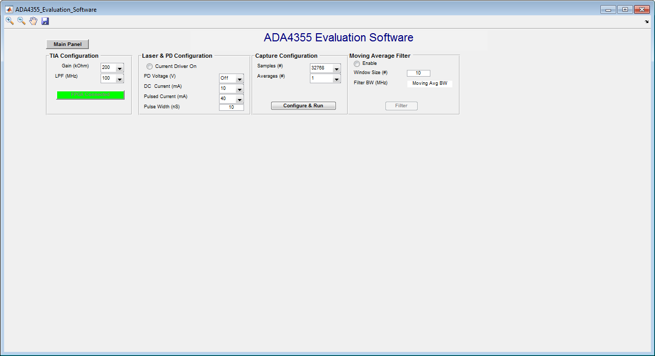
There are two panels: Main Panel and FFT Panel. The Main Panel controls the following settings:
Gain drop down menu is used to set the gain of the TIA.
LPF drop down menu is used to set the Analog Low Pass Filter inside the ADA4355.
Current Driver On radio button is used to enable or disable the laser driver from pulsing the laser.
PD Voltage drop down menu is used to set the Reverse Bias Voltage of the Photo Detector when using the on-board APD bias generator.
DC Current drop down menu is used to set the DC current through the laser diode. This biases the laser to a threshold level just below the current level where the laser would begin to emit light. The default and recommended level for the included laser diode is 10 mA.
Pulsed Current drop down menu is used to set the pulsed current through the laser diode.
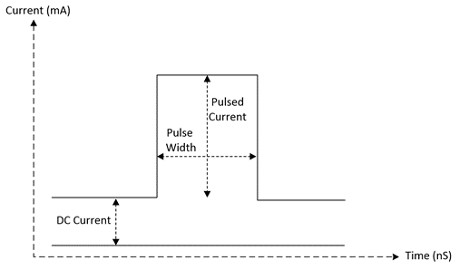
Pulse Width is the width of the optical pulse launched into the fiber. This setting is in steps of 2 ns and cannot exceed 20 us.
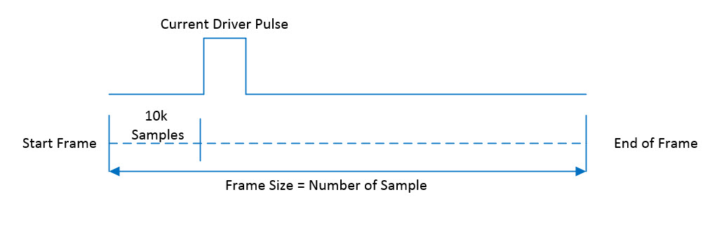
Samples drop down menu specifies the number of samples to be collected for each pulse. The samples collected are referred to as a “Frame”.
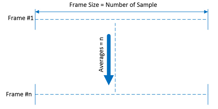
Averages drop down menu is used to set the number of data frames averaged for the measurement result.
Configure & Run is used to start the measurement any time measurement settings are changed.
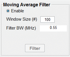
Enable is used to enable a moving average filter on the collected data.
Window Size sets the number of samples in the moving average filter.
Equivalent BW is the bandwidth of the moving average filter and is shown for convenience.
Making a Measurement
Once the measurement configurations are selected, click the Configure & Run button. A pop-up window is displayed with the remaining time of the measurement. Once the data is collected it is plotted as shown below.
Moving Average Filter
Once the measurement is done and the data is plotted, checking the Enable radio button will apply a moving average filter on the data. Change the Window Size and click the Filter button to update the filter window size (number of samples averaged).
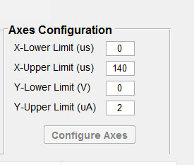
Axes Configuration
The Axes Configuration panel allows setting the axis limits. The X-Lower Limit and X-Upper Limit set the lower and upper x-axis limits respectively. The Y-Lower Limit and Y-Upper Limit set the lower and upper y-axis limits respectively.
When any changes are made in the Axes Configuration panel the Configure Axes button is enabled and must be clicked for the changes to take place.
Cursors
In the top left corner of the plot, the Cursors radio button enables two vertical cursors to appear on the plot. When the Cursors radio button is checked, the cursors data is displayed underneath the legend. The X and Y location of the cursors is shown as well as the delta X, delta Y, and ratio of the two deltas.
To slide the cursor, click and hold on the intended cursor and move the mouse to the intended location. By default, the cursors are tracking the raw data (blue curve). To track the filtered data (orange curve), click anywhere on the filtered data. The filtered data momentarily flashes and the color of the vertical cursor lines changes to match the color of the data trace they are tracking.
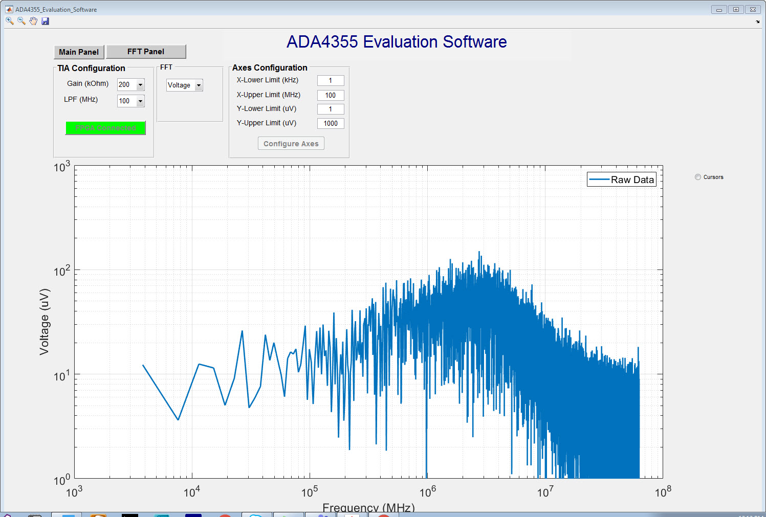
FFT Panel
Once data is collected, the FFT Panel tab appears at the top of the main panel. Click the FFT Panel tab; an FFT is run on the data and the FFT result appears.
Tool Bar
The Tool Bar is located on the top left corner of the GUI. Selecting the Zoom-in toggle and clicking on the plot will zoom in and center at the mouse location. Alternatively, click and drag to draw a box around the area to zoom. When the mouse button is released the axes zoom in to the region enclosed by the box.
The Zoom-out toggle works in the same manner but zooms out. Each mouse click zooms in or out by a factor of 2. While Zoom in or Zoom out is enabled, right click on the main plot and select Reset to Original View to go back to the original axes limits.
The Pan toggle (hand) turns on the pan mode for axes in the main plot. The Save toggle (floppy disk) saves the Raw Voltage data sampled by the ADC.
For Application Board Users Only
D23 in the FMC Connector, which is labeled as “1P8VA_EN”, needs to be driven by more than 1.2 V to make the ADA4355 Application board work properly.