EVAL-AD9213
12-Bit, 6 GSPS/10.25 GSPS, JESD204B, RF Analog-to-Digital Converter.
Overview
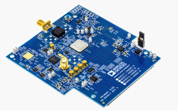
The EVAL-AD9213 is the evaluation board for the AD9213, a single, 12-bit, 6 GSPS/10.25 GSPS radio frequency (RF) analog-to-digital converter (ADC). The AD9213 supports high dynamic range frequency and time domain applications requiring wide instantaneous bandwidth and low conversion error rates. It features a 16-lane JESD204B interface to support maximum bandwidth capability.
Its integrated input buffer supports up to 6.5 GHz of input bandwidth and on-chip calibration and dithering preserve linearity and spurious-free performance across a wide range of signal conditions. A built-in digital downconverter (DDC) lets you tune to a specific frequency band and reduce the output data rate when full instantaneous bandwidth is not needed.
The evaluation board interfaces with an FPGA carrier via an FMC+ connector, using the AMD Xilinx VCU118 as the main supported platform, while the ADS8-V1EBZ capture board is also supported (limited).
Features:
High instantaneous dynamic range with low noise
Low power dissipation: <4.6 W typical at 10 GSPS
Wide 6.5 GHz input bandwidth with integrated input buffer
Overvoltage-protected analog input
16-lane JESD204B output interface (up to 16 Gbps line rate)
Multichip synchronization with 1 sample accuracy, including DDC NCO synchronization
Integrated digital downconverter (DDC) with selectable decimation
Fast frequency hopping via 48-bit NCO with 16 profile settings
Fast overrange detection for efficient AGC
On-chip temperature sensor and negative voltage generators
Low conversion error rate (CER)
Compact 12 mm × 12 mm, 192-ball BGA-ED package
Applications:
Wideband radar and electronic warfare (EW)
Test and measurement instrumentation
Wideband communications receivers
Direct RF sampling systems
Recommendations
People who follow the flow that is outlined, have a much better experience with things. However, like many things, documentation is never as complete as it should be. If you have any questions, feel free to ask on our EngineerZone, but before that, please make sure you read our documentation thoroughly.
To better understand the AD9213, we recommend using the EVAL-AD9213 evaluation board together with the AMD Xilinx VCU118 FPGA development kit or the ADS8-V1EBZ FPGA-based capture board.
Table of contents
Using the evaluation board/full stack reference design that we offer:
Prerequisites - what you need to get started
-
Using the AMD Xilinx VCU118/UltraScale+
Using the ADS8-V1EBZ with the AD9213-10GEBZ-B
Linux Applications
Design with the AD9213
-
AD9213 product page
Resources for designing a custom AD9213-based platform software
For Linux software:
About the device driver:
About the JESD204 utilities:
HDL reference design which you must use in your FPGA.
-
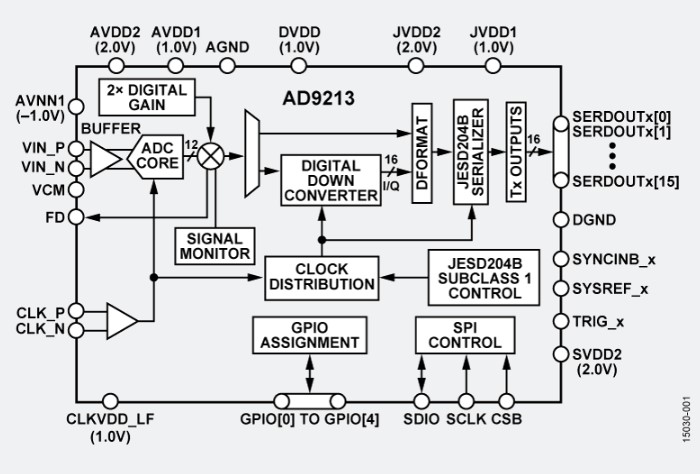
Block diagram
ADI articles
About the JESD204 standard:
Warning
All the products described on this page include ESD (electrostatic discharge) sensitive devices. Electrostatic charges as high as 4000V readily accumulate on the human body or test equipment and can discharge without detection. Although the boards feature ESD protection circuitry, permanent damage may occur on devices subjected to high-energy electrostatic discharges. Therefore, proper ESD precautions are recommended to avoid performance degradation or loss of functionality. This includes removing static charge on external equipment, cables, or antennas before connecting to the device.