User guide
Hardware guide
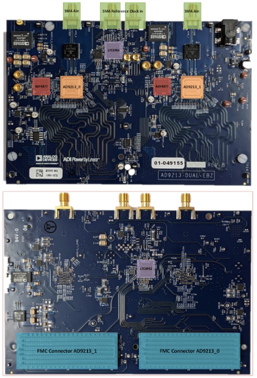
Evaluation board
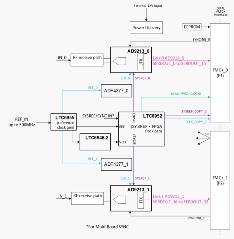
Scalable clocking architecture
The EVAL-AD9213-DUAL-EBZ implements a clocking architecture designed for multi-channel scalability. The ADF4377 ultra-low jitter PLL with integrated VCO generates the sample clock, while the LTC6955 low jitter fanout clock buffer and the LTC6952 JESD204B clock generation and distribution IC distribute clocks across both AD9213 converters. This architecture supports multi-chip synchronization (MCS) at 10 GSPS and enables the interleaved 20 GSPS operating mode.
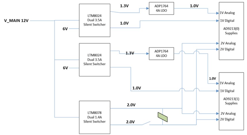
Power distribution network
Downloads
Description |
Download |
|---|---|
Schematic |
|
Layout |
|
BOM |
Software guide
The EVAL-AD9213-DUAL-EBZ is supported through the Linux IIO subsystem when used with the Intel Stratix 10 SX SoC Development Kit. The FPGA is programmed via the Quartus Prime Programmer and the system boots from an SD card containing the ADI Linux image.
Once booted, the following IIO-based tools can be used to interact with and capture data from the device:
All the products described on this page include ESD (electrostatic discharge) sensitive devices. Electrostatic charges as high as 4000V readily accumulate on the human body or test equipment and can discharge without detection. Although the boards feature ESD protection circuitry, permanent damage may occur on devices subjected to high-energy electrostatic discharges. Therefore, proper ESD precautions are recommended to avoid performance degradation or loss of functionality. This includes removing static charge on external equipment, cables, or antennas before connecting to the device.