EVAL-ADBMS2950-BASIC User Guide
Overview
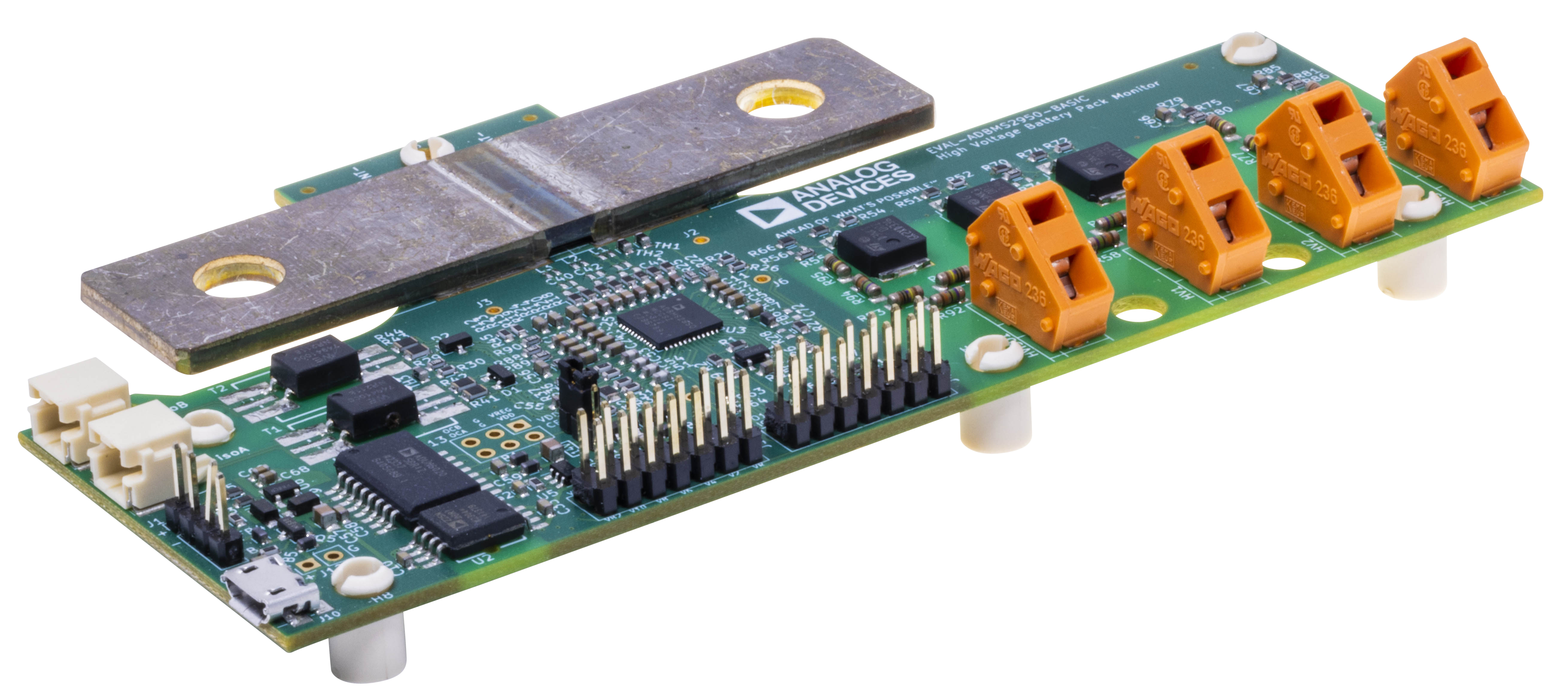
The EVAL-ADBMS2950-BASIC battery pack monitoring evaluation board features the ADBMS2950B, a bidirectional current monitor, with 12 buffered high impedance voltage sense inputs, linked through a 2-wire isolated serial interface (isoSPI™). The demo circuit also features reversible isoSPI™ enabling a redundant communication path.
The EVAL-ADBMS2950-BASIC can communicate to a PC over isoSPI™ by attaching an EVAL-ADBMS6822 dual-controller isoSPI™ add-on board to the expansion headers of an EVAL-SDP-CK1Z microcontroller and then connecting this MCU to a host PC through USB.
The EVAL-ADBMS2950-BASIC board can be operated on the same isoSPI™ daisy-chain with other ADBMS2950B and ADBMS6830B devices.
Features
Fully featured evaluation board for ADBMS2950B
Bidirectional high accuracy current measurement with on-board shunt
Increased input range overcurrent measurement and alert
Battery stack measurements such as
Battery stack voltage monitoring
Isolation measurement
Pre-charge monitoring
Fuse monitoring
Charger monitoring
Link voltage monitoring
Includes two isoSPI ports for daisy chain and reversible isoSPI support. The isoSPI connections can be done via simple DuraClik connectors.
Applications
Mobile Robot Systems
E-scooter/E-bikes/Light Electric Vehicle
Power Tools
Portable Energy Storage System
Backup Battery Systems
Grid Energy Storage
Performance Summary
Parameter |
Type |
Min |
Typ |
Max |
Unit |
|
|---|---|---|---|---|---|---|
Low-Voltage Power Supply Input |
||||||
Wide Range LV Input (J1) |
PIN |
6 |
15 |
V |
||
Alternative 5 V LV Input (J10, J12) |
PIN |
4.5 |
5.5 |
V |
||
Low-Voltage Digital Outputs |
||||||
Overcurrent Alert LVOCA, LVOCB |
DOUT |
0 |
5.5 |
V |
||
High-Voltage Shunt Sense Input |
||||||
Current |
AIN |
−131 |
131 |
mV |
||
Overcurrent |
AIN |
−300 |
300 |
mV |
||
Shunt Resistance |
50 |
μΩ |
||||
High-Voltage Power Supply Output |
||||||
VDD to GND |
POUT |
14 |
V |
|||
VREG to GND |
POUT |
5 |
V |
|||
High-Voltage Analog Input |
||||||
HVISO1 to GND |
HVIN |
0 |
1000 |
V |
||
HV1 to GND |
HVIN |
0 |
1000 |
V |
||
HV2 to GND |
HVIN |
−1000 |
1000 |
V |
||
HV3 to GND |
HVIN |
−1000 |
1000 |
V |
||
HV to LV Isolation |
||||||
GND to LGND |
1000 |
V |
PIN : Power Input ; POUT: Power Output
AIN : Analog Input ; DOUT
HVIN : High-Voltage Input
System Architecture
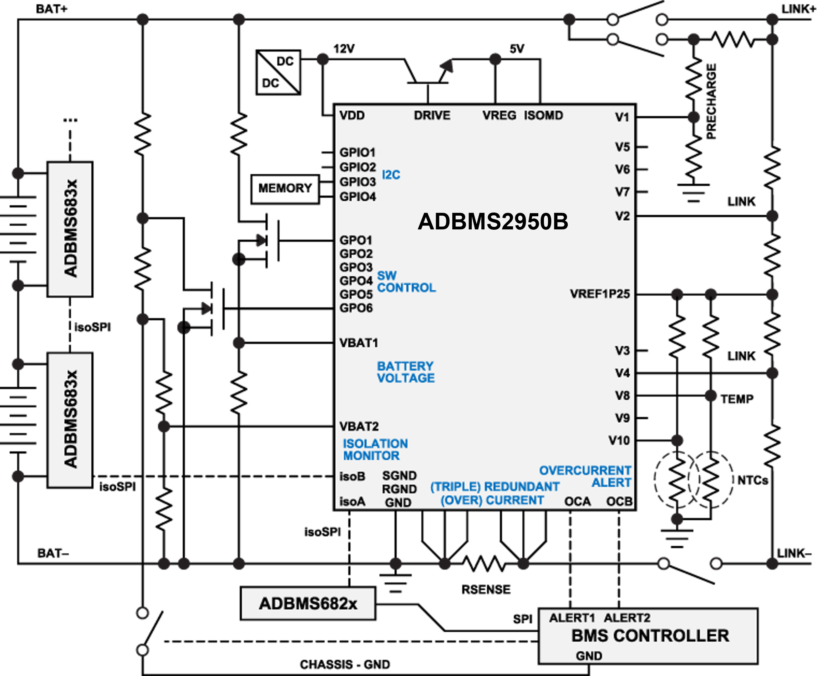
Components and Connections
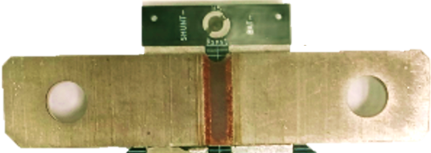
Current Sense Resistor
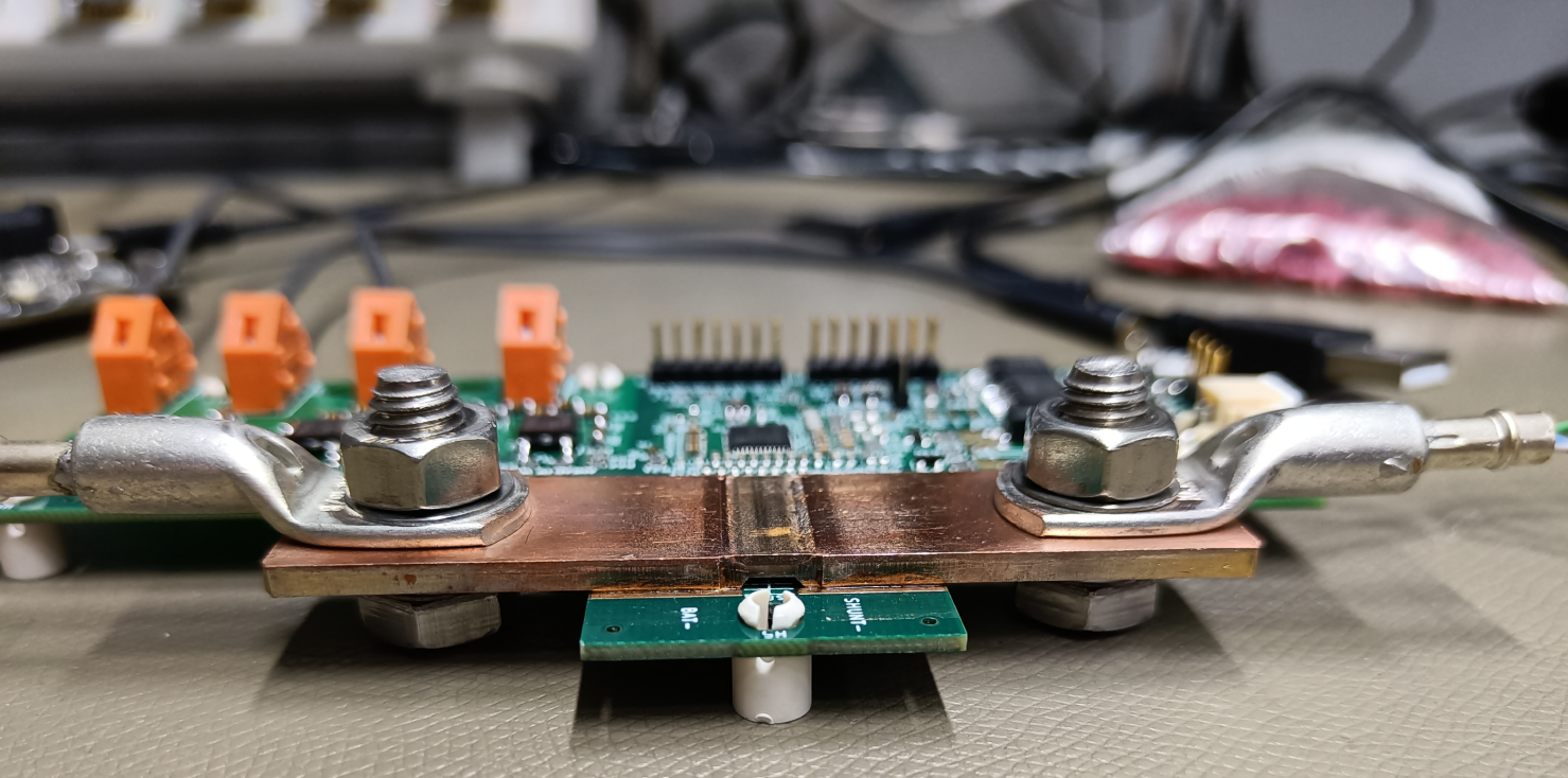
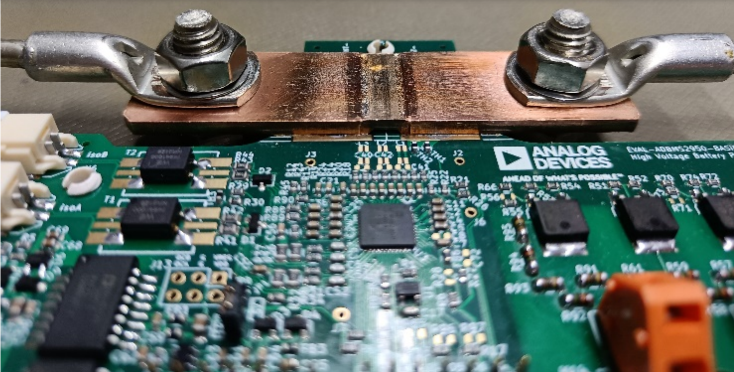
The EVAL-ADBMS2950-BASIC is equipped with a high-current bus bar style current sense resistor BAS-M-R00005-AE-5.0 from Isabellenhuette.
High Voltage Sense Inputs
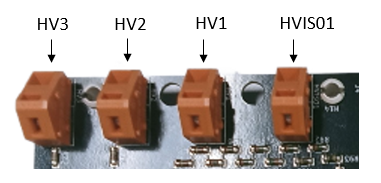
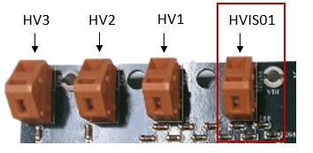
The EVAL-ADBMS2950-BASIC comes equipped with 4 clamps that allow application and monitoring of high input voltages up to 1000 V. The high-voltage input clamps are marked HVISO1, HV1, HV2, and HV3.
HV1: Battery Stack Voltage Input
The HV1 input is connected to 2 on-board voltage dividers to enable redundant monitoring of the full battery stack voltage and to perform LV to HV isolation resistance measurement.
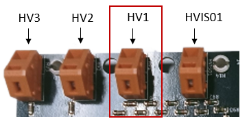
The voltage dividers transform the high input voltage applied to HV1 to the VB1ADC and VB2ADC input range. The voltage dividers connect to the VBAT1 and VBAT2 inputs of ADBMS2950B and thus to VB1ADC and VB2ADC, respectively. The VBAT1 and VBAT2 voltage sense nodes are not biased via VREF1P25, thus the allowed HV1 input voltage range is positive only (0 V to 1000 V).
HV2, HV3: Auxiliary High-Voltage Inputs
The EVAL-ADBMS2950-BASIC features 2 additional high-voltage inputs, HV2 and HV3, that are transformed into the input ranges of the V1ADC and V2ADC.
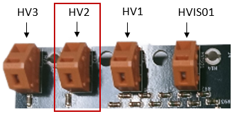
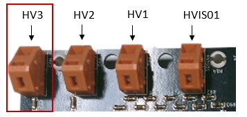
The HV2 and HV3 inputs enable the monitoring of high voltages in the battery system, such as LINK, FUSE, PRECHG and DCFC HV2 and HV3 are mapped to the ADBMS2950B inputs V2 and V3, respectively.
The V2 and V3 voltage sense nodes are biased to 1.25 V (VREF1P25), therefore the allowed input range of the HV2 and HV3 inputs is -1000 V to +1000 V.
HVISO1: Chassis-GND connection for Isolation Measurements
HVISO1 is a special-function input that is used to evaluate isolation measurements using the EVAL-ADBMS2950-BASIC. In order to conduct isolation measurements, the HVISO1 input shall be connected to chassis-GND through a controllable switch.
Auxiliary I/O Headers
The EVAL-ADBMS2950-BASIC features 2 headers, J4 and J5, that make available the ADBMS2950B voltage inputs, GPO, GPIO and power outputs for probing and as additional inputs and outputs.
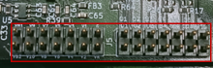
The following signals on the auxiliary headers J4 and J5 may be used as additional inputs and outputs:
Vx |
GPIO |
GPO |
V1 |
GPIO1 |
GPO4 |
V4 |
GPIO2 |
GPO5 |
V5C |
GPO6 |
|
V6C |
||
V8C |
||
V10C |
||
IMPORTANT: If voltage inputs of the auxiliary IO headers J4 and J5 are used the measured voltage signals must be transformed into the input range of the ADBMS2950 V1ADC and V2ADC, respectively. Thus, external resistive dividers similar to those used for HV1 to HV3 are required for measuring high voltage signals. |
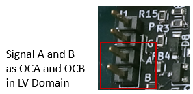
Overcurrent Outputs in Low-Voltage Domain
The ADBMS2950B overcurrent outputs OCA and OCB are transferred from the high-voltage domain into low-voltage using the ADuM225. They are available as signals A and B at the header J1.
2kB On-Board EEPROM
The EVAL-ADBMS2950-BASIC features a Microchip 24LC02B 2kB I2C EEPROM connected to the ADBMS2950B’s on-chip peripheral controller interface via pins GPIO3 and GPIO4.
The on-board EEPROM may be used as a persistent data storage, e.g., shunt resistor calibration information.
isoSPI™ Connectors
The EVAL-ADBMS2950-BASIC features 2 transformer-isolated isoSPI™ connectors enabling fully redundant reversible isoSPI™ functionality.
The isoSPI™ DuraClik cable supplied with the EVAL-ADBMS2950-BASIC may be plugged into any of the connectors J8 or J9, marked isoA and isoB, respectively.
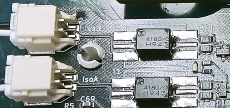
An evaluation board featuring another ADBMS2950B or ADBMS6830B device may be connected to the second isoSPI™ connector to build an isoSPI™ daisy-chain. Due to the reversible isoSPI feature, swapping connection from isoA to isoB is also possible.
Voltage Sense Overview
Below table shows the assignments of the voltage inputs to the ADBMS2950B pins and ADCs.
Name |
Enable |
ADBMS2950B Pin |
ADC |
HV1 (BAT+) |
GPO2 |
VBAT1 |
VB1ADC |
GPO1 |
VBAT2 |
VB2ADC |
|
HVISO1 |
GPO1 |
VBAT2 |
VB2ADC |
HV2 |
V2 |
V1ADC, V2ADC |
|
HV3 |
V3 |
V1ADC, V2ADC |
|
NTC1 |
V7 |
V1ADC |
|
NTC2 |
V9 |
V2ADC |
Remote Shunt
The EVAL-ADBMS2950-BASIC features unpopulated filter and protection circuitry for evaluation of remote shunt operation as per the ADBMS2950B data sheet.
In order to convert an EVAL-ADBMS2950-BASIC for remote shunt sensing, run through the following modifications:
On-board Shunt Removal
Remove the sense shunt resistor and solder on wires between the sense pads and the remote shunt.
Common-mode Choke Bypass
Cut the bypass traces of the footprints for the common-mode chokes. In the board schematics, you can find these at CURRENT SENSE SHUNT > optional common mode filter.
Populate the common-mode chokes. The EVAL-ADBMS2950-BASIC was designed to accept a Würth Elektronik WE-SL2 SMT Common-mode Line Filter.
TVS Protection Diodes
Unpopulated footprints for TVS diodes in SOT-23 package are located on the bottom layer of the EVAL-ADBMS2950-BASIC. The respective part in the schematics is located at CURRENT SENSE SHUNT > Optional TVS for remote shunt.
Power Supply
Type |
Ref |
Voltage |
Notes |
Power Header |
J1 |
6 V to 15 V |
Wide range supply input J1 Apply positive terminal of voltage source to pin marked + (LVCC, pin 1) Apply negative terminal of voltage source to pin marked - (LGND, pin 2) |
USB micro B plug |
J10 |
5 V |
Alternative 5 V supply input via USB |
LDO bypass power header |
J12 |
4.5 V to 5.5 V |
Alternative 5 V supply input via pin header |
Important
J10 and J12 bypass the on-board LDO used for the wide range supply input and instead connect directly to the ADuM6020 isolated power supply module.
J1 power input is connected to an ADP7142 LDO to regulate input voltage to 5V and as input overvoltage protection. Do not operate above 15V for extended periods of time to keep the ADP7142 within thermal limits.
Hardware Setup
Attachment of Cable Lugs to Shunt Resistor
The cable lugs must be attached to the shunt resistor with high force using a wrench on the top. When doing so, a wrench should also be attached to the hex screw head at the bottom to prevent it from rotating and thus putting too much force on the PCB.
Important
The contact surfaces of the shunt resistor and cable lugs should be polished and cleaned before attaching them. Oxidation and residue may increase contact resistance and heat dissipation.
The lug connectors are used to connect the 50 µΩ current measurement shunt to the load and the battery.
Large gauge wires should be used for this connection.
For several hundreds of Amperes, copper cables with a diameter of at least 10mm (AWG000) are recommended.
Bigger cables or using more than one in parallel will help minimize power dissipation and overheating.
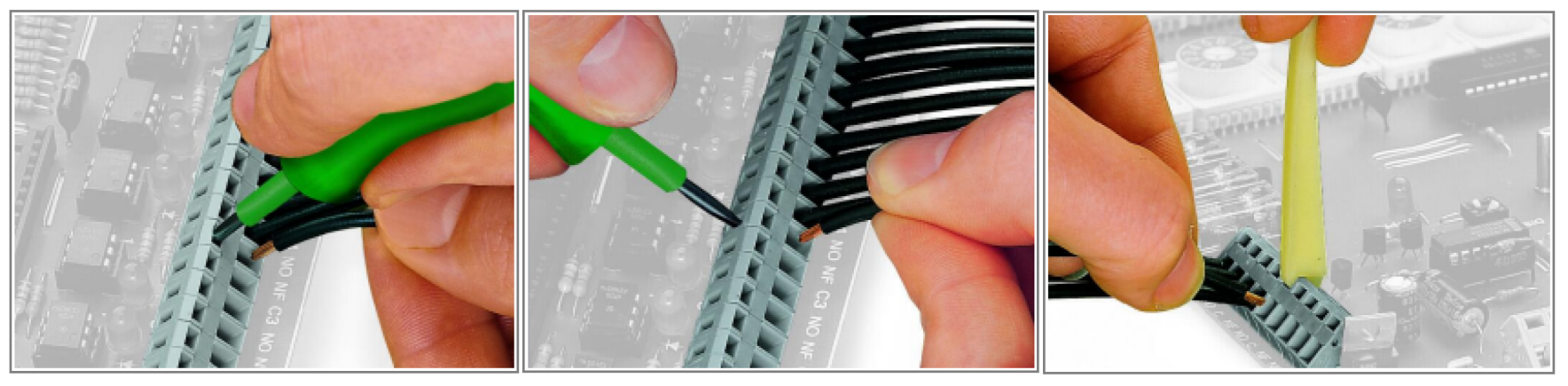
Connecting High-Voltage Input Clamps
The operation of the high-voltage clamps HVISO1, HV1, HV2, and HV3 is described in the ADBMS2950B datasheet.
A small flat-head screwdriver of 3.5mm bit width is required to operate the high-voltage clamp. To connect a wire to the clamp, loosen the clamp with the screwdriver, insert the wire and tighten the clamp as shown below:
Resources
Tip
Learn how to use the EVAL-ADBMS2950-BASIC board in conjunction other ADI BMS Modules. Visit the AD-CELLPACKBM-SL Hardware User Guide.
For Software Setup instructions, visit the EVAL-ADBMS2950-BASIC Software User Guide.
Design & Integration Files
Download
EVAL-ADBMS2950-BASIC Design & Integration Files
Schematic
PCB Layout
Bill of Materials
Allegro Project
Help and Support
Hint
For questions and more information, please visit the Analog Devices EngineerZone Support Community.
End of Document