User Guide
Hardware guide
Hardware configuration
The ADAQ8092 uModule soldered to the EVAL-ADAQ8092-FMCZ does not require an external supply to power up the board. It uses the +12 V supply from the carrier board (such as ZedBoard) and activates the on-board LDOs to provide the 3.3 V and 1.8 V supplies needed by the board.
On the ZedBoard, configure the BOOT switches (JP7-JP11) and the MIO0 jumper (JP6) for the desired boot mode, and set VADJ to 2.5 V as required by the HDL project. Refer to the ZED Quickstart guide for the specific jumper positions for SD card and JTAG boot modes.
Analog Inputs

The EVAL-ADAQ8092-FMCZ allows the user to use either a single-ended or differential source. For single-ended input, the user can either use the on-board balun to drive the part differentially, or bypass it to drive the part in single-ended mode. The input configuration is selected using jumper settings and 0 Ohm resistor placement.
Factory default settings (single-ended input)
Channel |
Link |
Location |
|---|---|---|
1 |
JP1 |
Pin 2 to Pin 3 |
JP3 |
Pin 2 to Pin 1 |
|
JP4 |
Pin 2 to Pin 3 |
|
2 |
JP2 |
Pin 2 to Pin 3 |
JP5 |
Pin 2 to Pin 1 |
|
JP6 |
Pin 2 to Pin 3 |
Note
With the factory default settings, the board is ready for a single-ended source. If using a differential source instead, install 49.9 Ohm resistors at R1 (Channel 1) and R3 (Channel 2) to properly balance the inputs.
Differentially driven using the balun
Channel |
Link |
Location |
|---|---|---|
1 |
JP1 |
Pin 2 to Pin 1 |
JP3 |
Pin 2 to Pin 3 |
|
JP4 |
Pin 2 to Pin 1 |
|
2 |
JP2 |
Pin 2 to Pin 1 |
JP5 |
Pin 2 to Pin 3 |
|
JP6 |
Pin 2 to Pin 1 |
Note
When using this configuration, resistor values must also be changed to properly balance the impedance and maintain a gain of approximately 5. For Channel 1: R8 and R9 = 200 Ohm, R14 and R16 = 18.2 Ohm. For Channel 2: R10 and R11 = 200 Ohm, R15 and R17 = 18.2 Ohm.
Encode circuitry

The board supports both single-ended and differential encode modes. The default configuration uses the single-ended encode mode, which requires a CMOS level signal. The board also provides an option to install an oscillator at Y1 as a built-in clock source for single-ended encode mode.
When using a sinusoidal, PECL, or LVDS signal, the differential encode mode is recommended.
Power supply

The EVAL-ADAQ8092-FMCZ uses the +12 V supply from the carrier board at pin C35 of the FMC connector. The power distribution chain is:
LTC4359 (U2): reverse input protection
LTM8074 (U4): step-down regulator, configured for 5 V output
LTC1673-1.8 (U3): provides VDD and OVDD supplies (1.8 V)
LTC1763-3.3 (VR1): provides VCC supply (3.3 V)
The VADJ voltage provided from the carrier through the FMC connector must be set to 2.5 V. The VADJ value can be checked in the HDL project at ADAQ8092-FMC HDL project.
External supplies can also be used if some of the built-in power circuitry requires rework.
Schematic
The evaluation board schematic can be found at:
ADI IIO Oscilloscope
The IIO Oscilloscope is a cross-platform application for interfacing with IIO devices, enabling you to configure device parameters and visualize data.
Important
Make sure to download/update to the latest version of IIO Oscilloscope.
For Linux
Remote run on host
The IIO Oscilloscope application can be used to connect to another platform that has a connected device, to configure the device and read data from it. This application is not for performance testing, but rather showcasing the basic features.
Please see IIO Oscilloscope documentation for installation steps and more details.
Build and start osc on a network-enabled Linux host.
For Windows computers, open the application from the start menu.
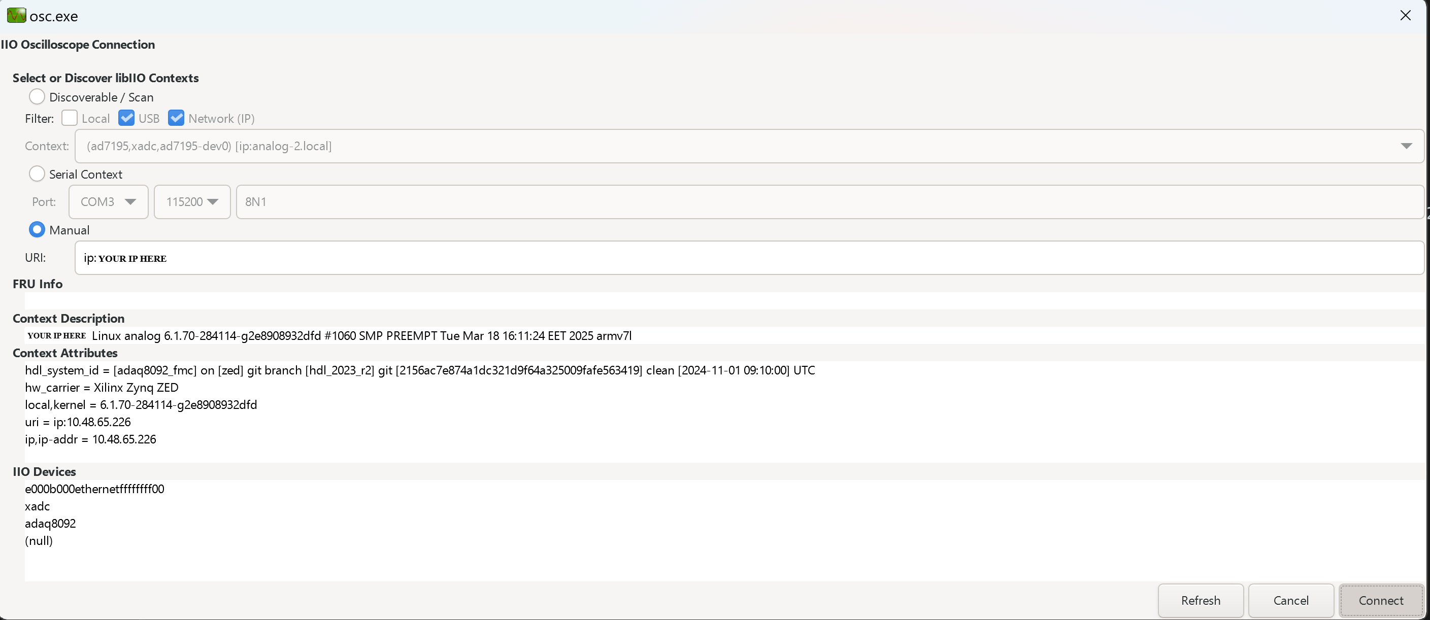
Once the application is launched, go to Settings > Connect > URI and type “ip:” then the IP address of the target in the pop-up window. This IP can be found out with a command from the previous section of this documentation.
Locally run on the board
If you connected an HDMI monitor to your FPGA and a mouse and a keyboard (both on one dongle), you can navigate the ADI Kuiper Linux that is on the FPGA.
Going to the top left corner icon (the menu icon), search for IIO Oscilloscope. Opening it will automatically connect to the setup and you can use the application.
For no-OS
For connecting IIO Oscilloscope to no-OS applications, they need to be built with the IIOD=y flag. This way, the no-OS applications will run an IIO daemon that is awaiting connections from the IIO Oscilloscope.
As indicated in the boot log, the board runs an IIOD server over the serial (UART) connection.
Disconnect or close the serial terminal used to view the boot log.
Once done with the installation or an update of the latest IIO Oscilloscope, open the application.
Select the Serial backend and configure the connection with the settings shown at the end of the boot log.
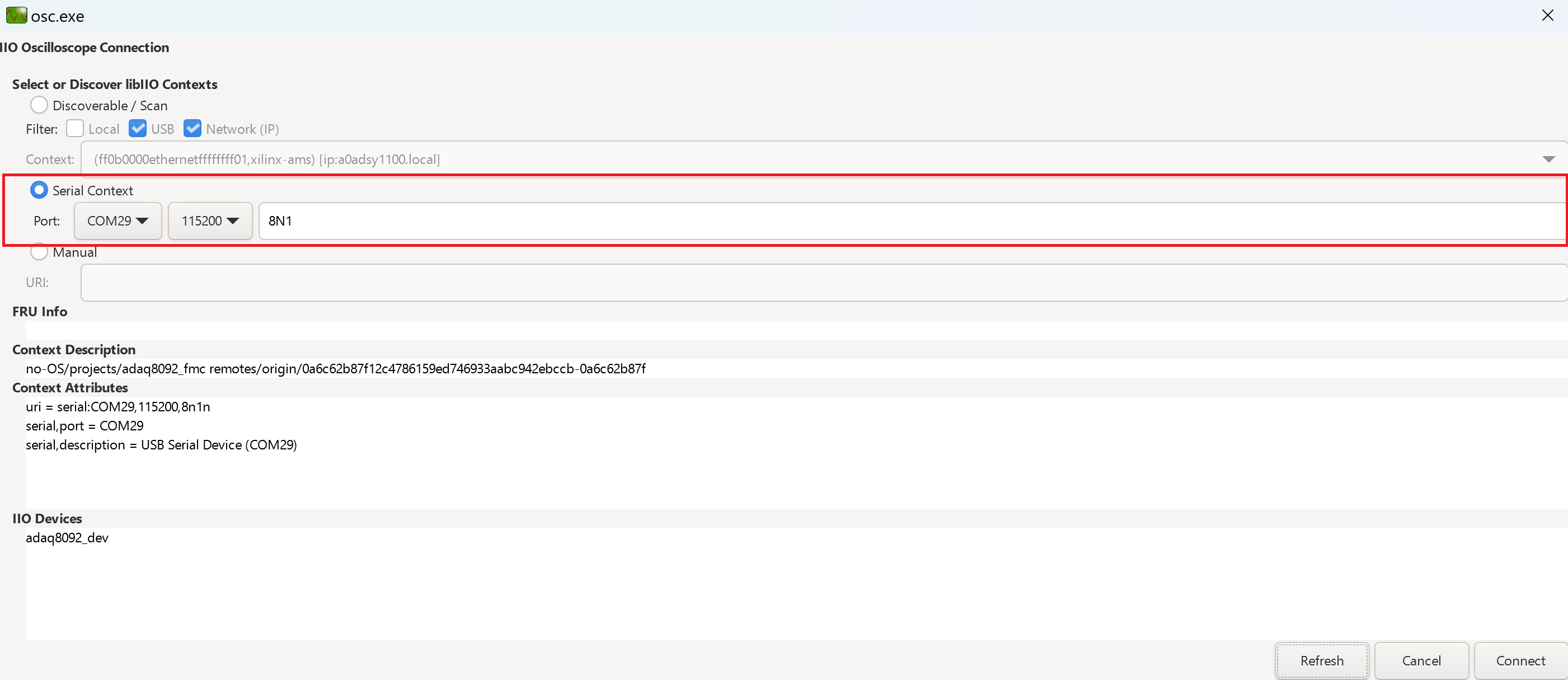
Press Refresh to display the available IIO devices and press Connect.
Note
The serial port is the COM port on Windows or /dev/ttyUSBx on Linux.
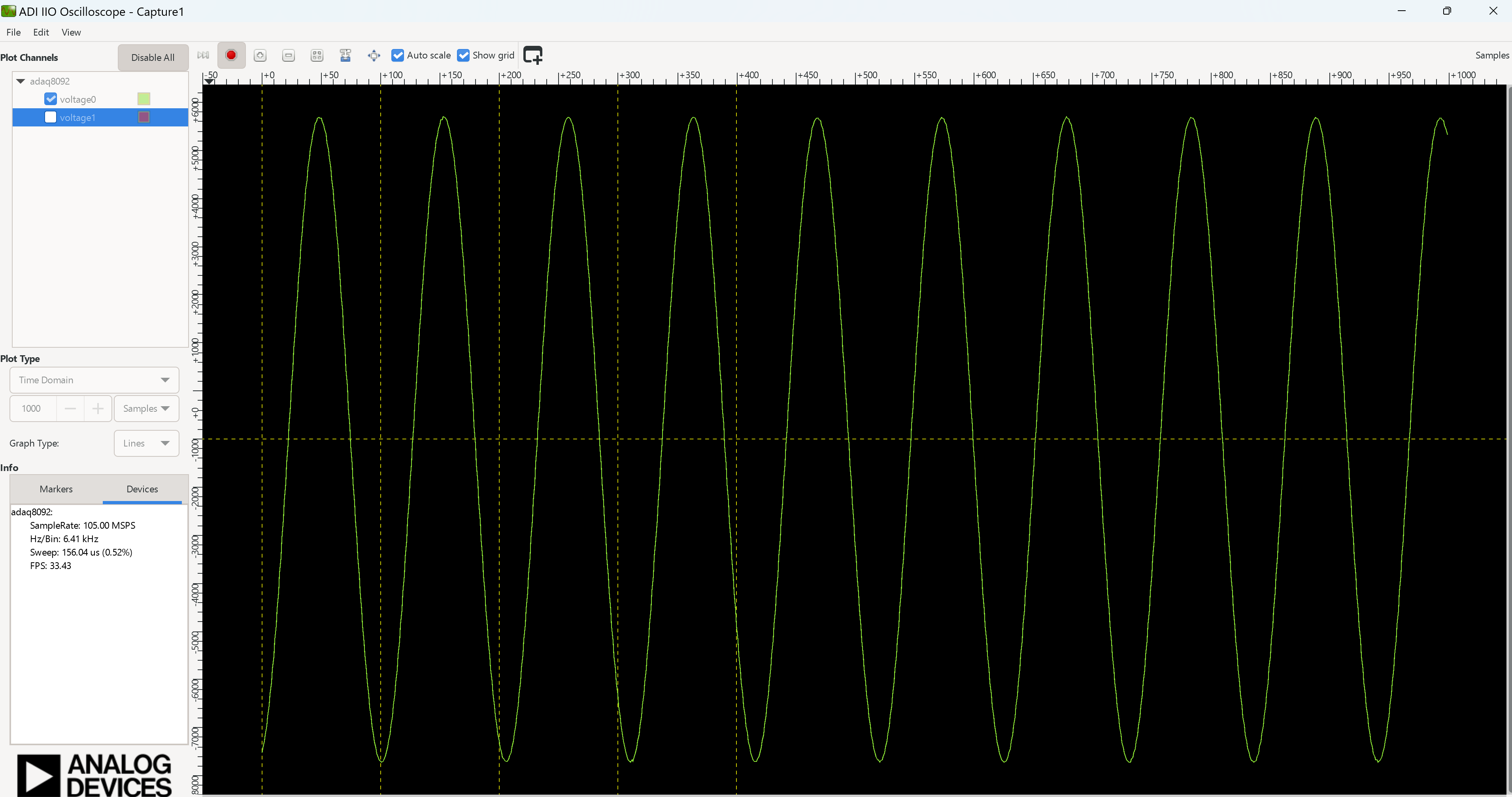
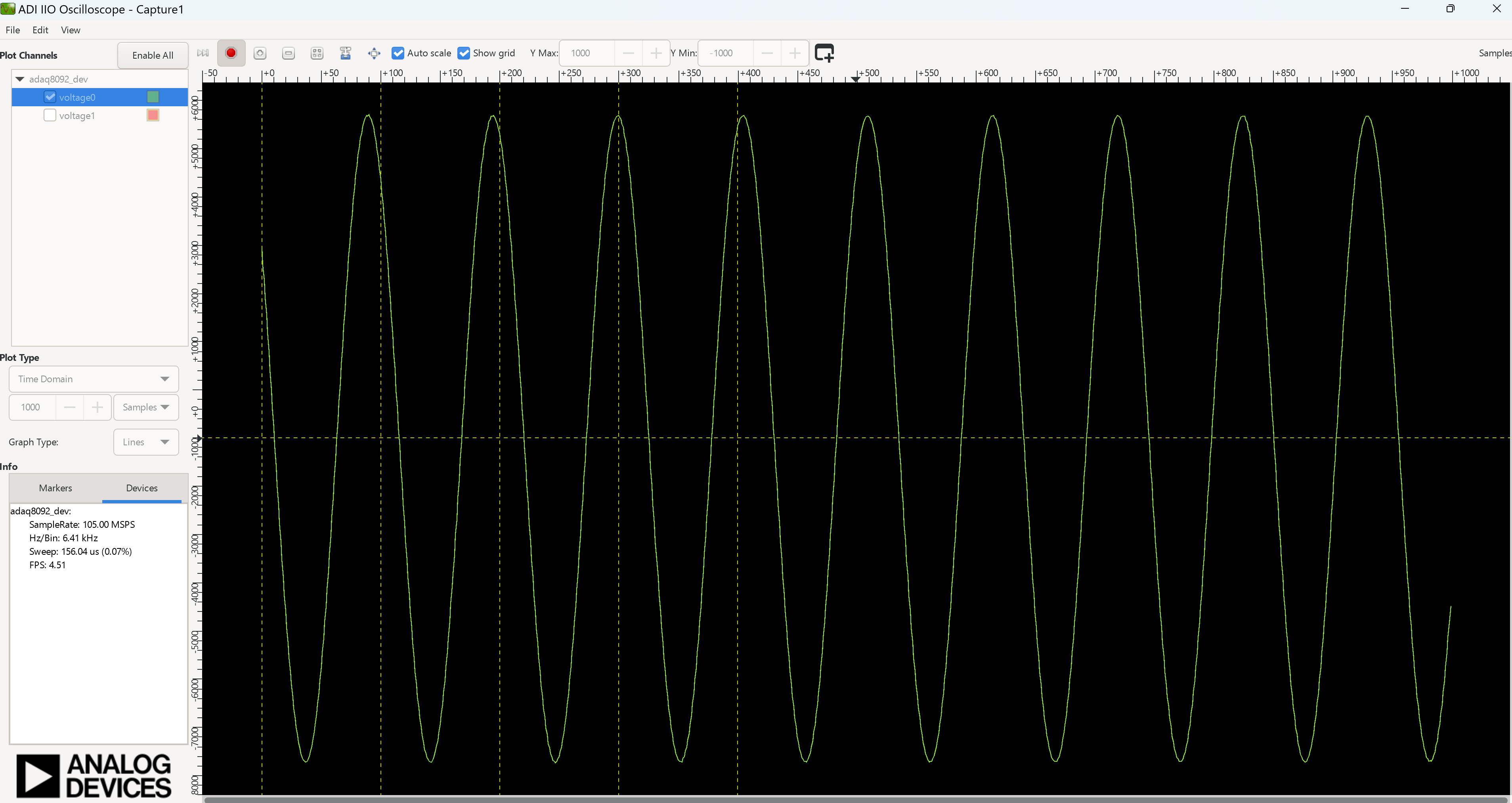
Data capture
Note
Device names and channel definition may differ between no-OS and Linux.
Linux
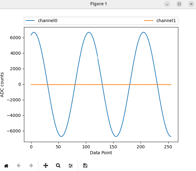
Time domain:
no-OS
Time domain:
Pyadi-IIO
PyADI-IIO is a python abstraction module for ADI hardware with IIO drivers to make them easier to use.
This module provides device-specific APIs built on top of the current libIIO python bindings. These interfaces try to match the driver naming as much as possible without the need to understand the complexities of libIIO and IIO.
Running the Example
After installing and configuring PYADI-IIO in your machine, you are now ready to run python script examples. In our case, run the adaq8092_example.py found in the examples folder.
Connect the EVAL-ADAQ8092 to the ZedBoard.
Open command prompt or terminal and navigate through the examples folder inside the downloaded or cloned pyadi-iio directory.
Run the example script using the command.
/path/to/pyadi-iio/examples$
python3 adaq8092_example.py
Before running the example, make sure to connect a signal generator and a clock source to the evaluation board as described in ZED Quickstart.
The expected output should look like this:
GitHub link for the python sample script: ADAQ8092 Python Example