Evaluating the ADAQ7768-1 24-Bit, Single Channel Precision μModule Data Acquisition System
Features
Evaluation kit for ADAQ7768-1 24-bit single-channel precision μModule data acquisition system
Switch or GPIO controlled gain mode
Complete power management solution
FMC connector to FPGA for digital interface
Optional Arduino and PMOD connector
Evaluation Kit Contents
EV-ADAQ7768-1FMC1Z evaluation board
Equipment Needed
SDP-H1 (EVAL-SDP-CH1Z) system demonstration platform
DC/AC signal source (Audio Precision or similar high performance signal source)
PC running Windows 7, 8, or 10 with USB 2.0 port
Software Requirement
ACE (Analysis, Control, Evaluation) software
General Description
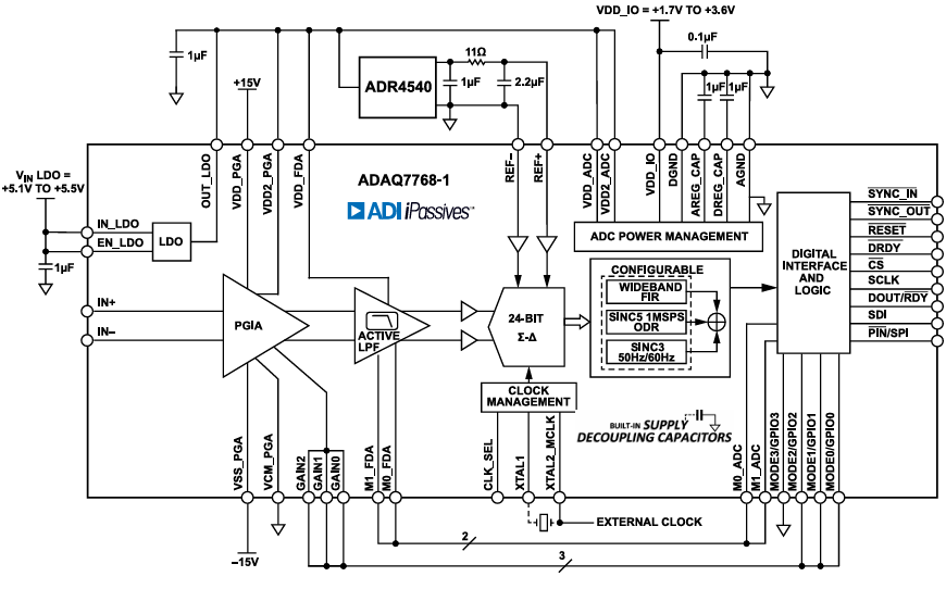
The EV-ADAQ7768-1FMC1Z evaluation kit features the ADAQ7768-1, a 24-bit, single-channel precision data acquisition system (DAQ) μModule system. The evaluation board demonstrates the performance of the ADAQ7768-1 μModule and is a versatile tool for a variety of applications.
The EV-ADAQ7768-1FMC1Z board connects to the USB port of the PC through the system demonstration platform (SDP-H1). By default, all the necessary supply rails on the EV-ADAQ7768-1FMC1Z are powered by a 3.3 V rail coming from the SDP-H1. The 3.3 V rail is regulated by the on-board power solution to ±15 V and 5.3 V to power the ADAQ7768-1 and its support components.
The EV-ADAQ7768-1FMC1Z is used alongside a downloadable evaluation software (ACE) that fully configures the ADAQ7768-1 device register functionality, and also provides DC and AC time and frequency domain analysis in the form of waveform graphs, histograms, and associated noise analysis for ADC performance evaluation. The ACE software controls the EV-ADAQ7768-1FMC1Z over the USB through the system demonstration platform (SDPH1).
The ADAQ7768-1 data sheet provides a full description and complete specifications of the ADAQ7768-1. Consult it in conjunction with this user guide when using the evaluation board. Full details on the SDP-H1 are available on the SDP-H1 product page.
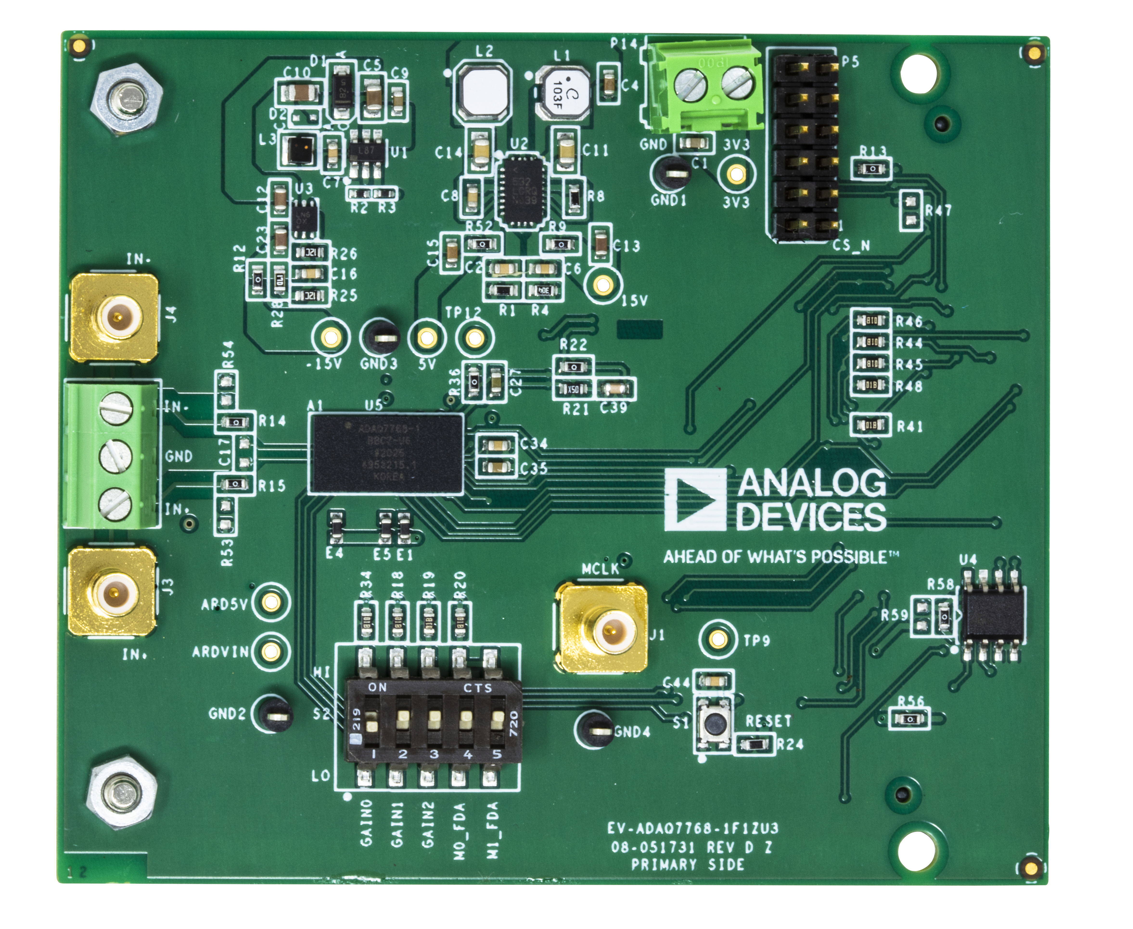
Evaluation Board Photograph
Quick Start Guide
To begin using the evaluation board, take the following steps:
Ensure the SDP-H1 system demonstration platform board is disconnected from the PC. Install the ACE (Analysis, Control, Evaluation) software to evaluate ADAQ7768-1. Restart the PC after the software installation is complete. For complete software installation instructions, see the Software Installation Procedures section.
Connect the SDP-H1 system demonstration platform board to the unpowered EV-ADAQ7768-1FMC1Z evaluation board. The J4 connector of the SDP-H1 system demonstration platform board connects to the receiving socket, P1, on the EV-ADAQ7768-1FMC1Z printed circuit board (PCB).
Ensure the evaluation boards are connected firmly together by screwing them together.
Connect the 12V DC supply to the SDP-H1 system demonstration platform board and then connect to the PC using the supplied USB cable. Choose to automatically search for the drivers for the SDP-H1 if prompted by the operating system.
Launch the ACE (Analysis, Control, Evaluation) software from the Analog Devices subfolder in the Programs menu.
To power off, first close the software. Then press the reset button on the SDP-H1 before disconnecting the power or USB.
Design Overview
Evaluation Board Hardware
Hardware Link Options
Table 1. Default Link and Solder Link Options
Name |
Link No. |
Default Link Option |
Description |
|---|---|---|---|
Differential/Single Ended Input |
R53 R54 |
DNI |
R53 set IN+ to ground for single ended input R54 set IN- to ground for single ended input |
ADR4540 Vin Select |
R23 R60 |
R23 |
Set the source for the voltage input for ADR4540 R23 set ADR4540 voltage input to the output of the LDO R60 set ADR4540 voltage input to 5.3V |
FDA Power Mode Input |
R10 R11 |
DNI |
Set the power mode selection to auto or manual selection R10 set the M1_FDA power mode input to manual selection R11 set the M0_FDA power mode input to manual selection |
S2 |
1A-1B 2A-2B 3A-3B 4A-4B 5A-5B |
Set the GPIO mode and FDA power mode 1A-1B set the GPIO0 to high or low 2A-2B set the GPIO1 to high or low 3A-3B set the GPIO2 to high or low 4A-4B set the M1_FDA power mode to low power mode or high power mode 5A-5B set the M0_FDA power mode to low power mode or high power mode |
On-Board Connectors
Table 2 provides information about the external on-board connectors on the EV-ADAQ7768-1FMC1Z.
Table 2. On-Board Connectors
Connector |
Function |
|---|---|
P1 |
Connects all digital signals to the SDP-H1 board |
P2/P3 |
Arduino header pads, not installed by default |
P5 |
PMOD connector block |
P14 |
DC analog inputs |
J3/J4/P7 |
SMB and Terminal Block connector for analog inputs, IN+, IN- |
S1 |
ADC reset switch |
S2 |
Mechanical switch for Gain and FDA power mode control |
J1 |
SMB connector for the external MCLK |
J2 |
SMB connector for the low voltage differential signaling (LVDS) clock on the XTAL1 pin |
Power Supplies
The evaluation board requires 3.3V power supply to operate. By default, the 3.3V rail is supplied by the SDP-H1, and the SDP-H1 is powered by a 12V wall adapter. The terminal block P14, can also be used to supply the evaluation board with 3.3V in case the user prefers to evaluate the EV-ADAQ7768-1FMC1Z with a third-party capture board.
The EV-ADAQ7768-1FMC1Z uses LT3095 (U2), a dual channel integrated boost and LDO regulator in a single package. LT3095 generates the +15V needed by the VDD_PGA pin of ADAQ7768-1 and a 5.3V to supply the built-in LDO of ADAQ7768-1. The LDO of the ADAQ7768-1 is used to power the VDD2_PGA, VDD_FDA, VDD_ADC, VDD2_ADC, and the ADR4540 reference device as shown on ADAQ7768-1 Datasheet Quick Start Up Guide.
ADP2300 (U1) is used to scale the 3.3V from SDP-H1 to -16V, while ADP7182 (U3), a low noise LDO, regulates the voltage to -15V which is used by the VSS_PGA.
The 3.3V from SDP-H1 is also used to supply the power needed on the VDD_IO.
Board Connection
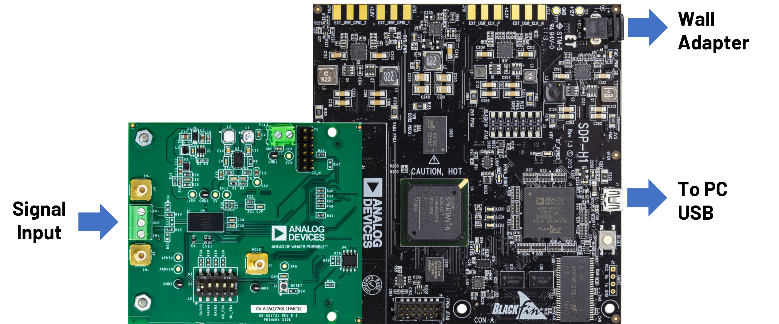
Follow the board connection shown in Figure 10. Connect the SDP-H1 with the 12V wall adapter and to PC through a USB cable.
Configuring the Evaluation and SDP Board
Connect the SDP-H1 to P1 on the EV-AD7768-1FMCZ board. Screw the two boards together.
Evaluation Board Software
Software Installation Procedures
Before using the EV-ADAQ7768-1FMC1Z, download and install the ACE (Analysis, Control, Evaluation) software. Download also the ADAQ7768-1 ACE plugin from the plugin manager, or from the EV-ADAQ7768-1FMC1Z product page.
ACE is a desktop software application that evaluates and controls multiple evaluation systems across the Analog Devices product portfolio. The installation process consists of the ACE Software Installation and the SDP-H1 driver installation.
Warning
Warning
To ensure the evaluation system is correctly recognized when it is connected to the PC, install the ACE software and SDP-H1 driver first before connecting the EV-ADAQ7768-1FMC1Z and SDP-H1 board to the USB port of the PC.
Installing the ACE Software
To install the ACE software, take the following steps:
Download the ACE software to a Windows-based PC.
Double-click the ACEInstall.exe file to begin the installation. By default, the software is saved to the following location: C:\Program Files (x86) \Analog Devices\ACE.
A dialog box appears asking for permission to allow the program to make changes to the PC. Click Yes to begin the installation process.
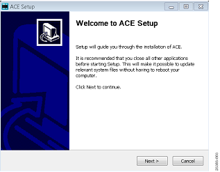
Click Next > to continue the installation, as shown in Figure 3.
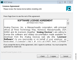
Read the software license agreement and click I Agree (see Figure 4).
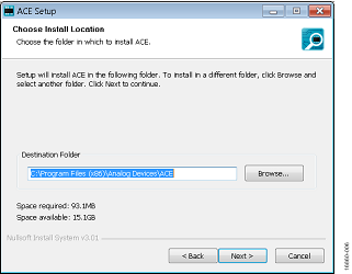
Choose an installation location and click Next (see Figure 5).
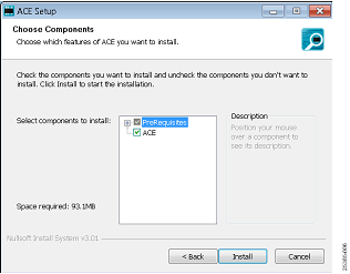
Select the Pre-Requisites checkbox to include the installation of the SDP-H1 driver. Click Install (see Figure 6).
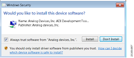
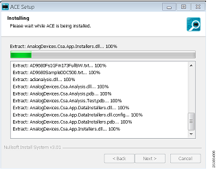
The Windows Security window appears. Click Install (see Figure 7). The installation is in progress. No action is required (see Figure 8).

The installation is complete (see Figure 9). Click Next > and then click Finish to complete.
Evaluation Board Setup Procedures
The EV-ADAQ7768-1FMC1Z connects to the SDP-H1. The SDP-H1 board serves as the communication link between the PC and the EV-ADAQ7768-1FMC1Z. Figure 10 shows a diagram of the connections between the EV-ADAQ7768-1FMC1Z and the SDP-H1 board.
Connecting the EV-ADAQ7768-1FMC1Z and the SDP-H1 to a PC
After installing the ACE software, take the following steps to set up the EV-ADAQ7768-1FMC1Z and the SDP-H1, as shown in Figure 10:
Ensure that all configuration links are in the appropriate positions, as detailed from Table 1.
Connect the EV-ADAQ7768-1FMC1Z securely to the 160-way connector on the SDP-H1. The EV-ADAQ7768-1FMC1Z does not require an external power supply adapter.
Connect the SDP-H1 to the PC via the USB cable and power it up with the 12V wall adapter included in the SDP-H1 kit
Setting Up the System for Data Capture
After completing the steps in the Evaluation Board Software section and the Evaluation Board Hardware section, set up the system for data capture as follows:
Run the Found New Hardware Wizard after the SDP-H1 system demonstration platform board is plugged into the PC. If using Windows XP, the user may need to search for the SDP-H1 drivers. Automatically search for the drivers for the SDP-H1 system demonstration platform board if prompted by the operating system.
Check that the evaluation board is connecting to the PC correctly using the Device Manager of the PC. Access the Device Manager as follows:
Right click My Computer and then click Manage.
A dialog box appears asking for permission to allow the program to make changes to the computer. Click Yes.
The Computer Management window appears. Click Device Manager from the list of System Tools (see Figure 11).
If the SDP-H1 system demonstration platform board appears under ADI Development Tools, the driver software is installed and the evaluation board is connecting to the PC correctly.
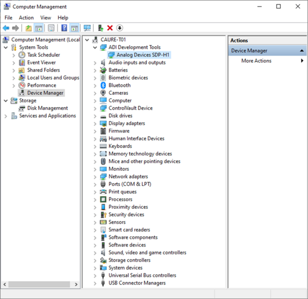
Figure 11 Checking that the Evaluation Board is connected to the PC correctly
Disconnecting the EV-ADAQ7768-1FMC1Z
Disconnect power from the SDP-H1 or press the reset tact switch located alongside the mini-USB port on the SDP-H1 before disconnecting the EV-ADAQ7768-1FMC1Z from the SDP-H1.
ACE Software Operation
Launching the Software
After completing the steps in the Setting Up the System for Data Capture section, take the following steps to launch the ACE software:
From the Start menu, select All Programs > Analog Devices > ACE > ACE.exe to open the main software window shown in Figure 12.
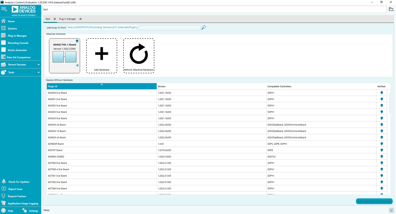
The EV-ADAQ7768-1FMC1Z icon appears in the Attached Hardware section.
If the EV-ADAQ7768-1FMC1Z is not connected to the USB port via the SDP-H1 board when the software is launched, the EV-ADAQ7768-1FMC1Z board icon does not appear in the Attached Hardware section. Connect the EV-ADAQ7768-1FMC1Z and SDP-H1 board to the USB port of the PC and wait a few seconds, then continue following these instructions.
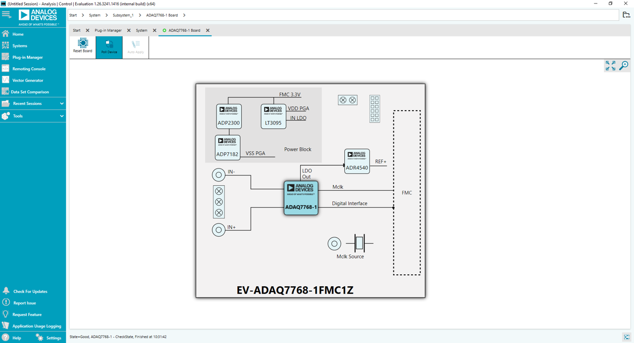
Double-click the EV-ADAQ7768-1FMC1Z board icon to open the window shown in Figure 13.
Double-click the EV-ADAQ7768-1FMC1Z chip icon to open the window shown in Figure 14.
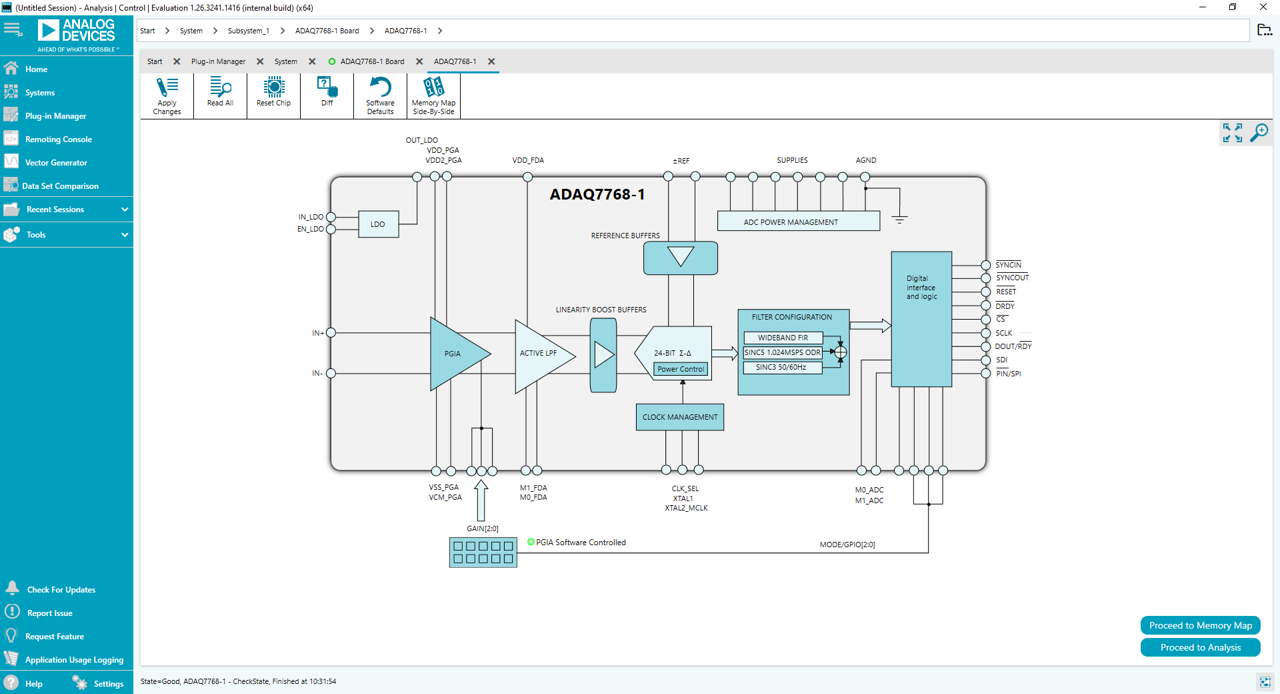
Click Software Defaults and then click Apply Changes.
Click Proceed to Analysis to open the EV-ADAQ7768-1FMC1Z analysis shown in Figure 15.
Startup Sequence
After running the software, the following sequence of events occurs:
The software accesses the EEPROM on the main evaluation board, which contains the board ID
Once the EEPROM value is verified, the PC loads the corresponding firmware to the FPGA on the SDP-H1.
After the loading of the firmware, the SDP-H1 supplies the 3.3V to the main evaluation board and establishes communication with the DUT.
The software then loads a preset of register values to the DUT’s user register map to configure the DUT to the tool’s default operating mode.
Description of the Analysis Window
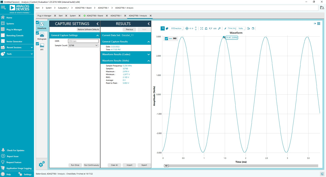
Click Proceed to Analysis in the chip view window to open the window shown in Figure 14. The Analysis view window allows the user to showcase the performance of the EV-ADAQ7768-1FMC1Z. Before performing any measurements, set the capture settings (see the CAPTURE SETTINGS section) and analysis settings (see the ANALYSIS section).
The Analysis view window contains the Waveform tab (see Figure 15), the Histogram tab (see Figure 16), and the FFT tab (see Figure 17).
Capture Settings
The General Capture Settings allows the user to configure the Sample Count and the ODR (Output Data Rate). These settings reflect in the registers automatically before data capture.
The Sample Count enables the user to select the number of samples per capture. The default value is set at 8192 samples, which can also be changed to the selection of the dropdown list, ranging from 512 to 131072 samples.
The ODR (Output Data Rate) is automatically calculated by the software based on the selected ADC filter settings. By default, this is set to 256 kSPS.
Click Run Once in the Capture Settings section to start a data capture of the samples at the sample rate specified in the Sample Count dropdown list. These samples are stored on the FPGA device and are only transferred to the PC when the sample frame is complete.
Click Run Continuously in the Capture Settings section to start a data capture that gathers samples continuously with one batch of data at a time. This operation runs the Run Once operation continuously.
Analysis
The General Settings section allows the user to set up the preferred configuration of the FFT analysis. This configuration sets the number of tones to be analyzed and the fundamental strategy to be used.
The Windowing section allows the user to set up the preferred windowing type to use in the FFT analysis. Other parameters that must be included in the analysis (i.e., number of harmonics, fundamental bins, harmonic bins, DC bins and worst other bins) can also be configured.
The Single Tone Analysis and the Two-Tone Analysis sections sets up the fundamental frequencies included in the FFT analysis. When one frequency is analyzed, use the Single Tone Analysis section. When two frequencies are analyzed, use the Two-Tone Analysis section.
Results
Click Export to export the captured data. The waveform, histogram, and FFT data is stored in .xml files along with the values of the parameters at capture.
Waveform Tab
The Waveform tab displays data in form of time vs. discrete data values with the results, as shown in Figure 15.
The data waveform graph shows each successive sample of the μModule output. The user can zoom in on and pan over the waveform graph using the embedded waveform tools above the graph.
Click the display unit’s dropdown list (shown with the Codes option selected in Figure 15) to select whether the data graph displays in units of hexadecimal, volts, or codes. The axis controls are dynamic.
When selecting either y-scale dynamic or x-scale dynamic, the corresponding axis width automatically adjusts to show the entire range of the μModule results after each batch of samples.
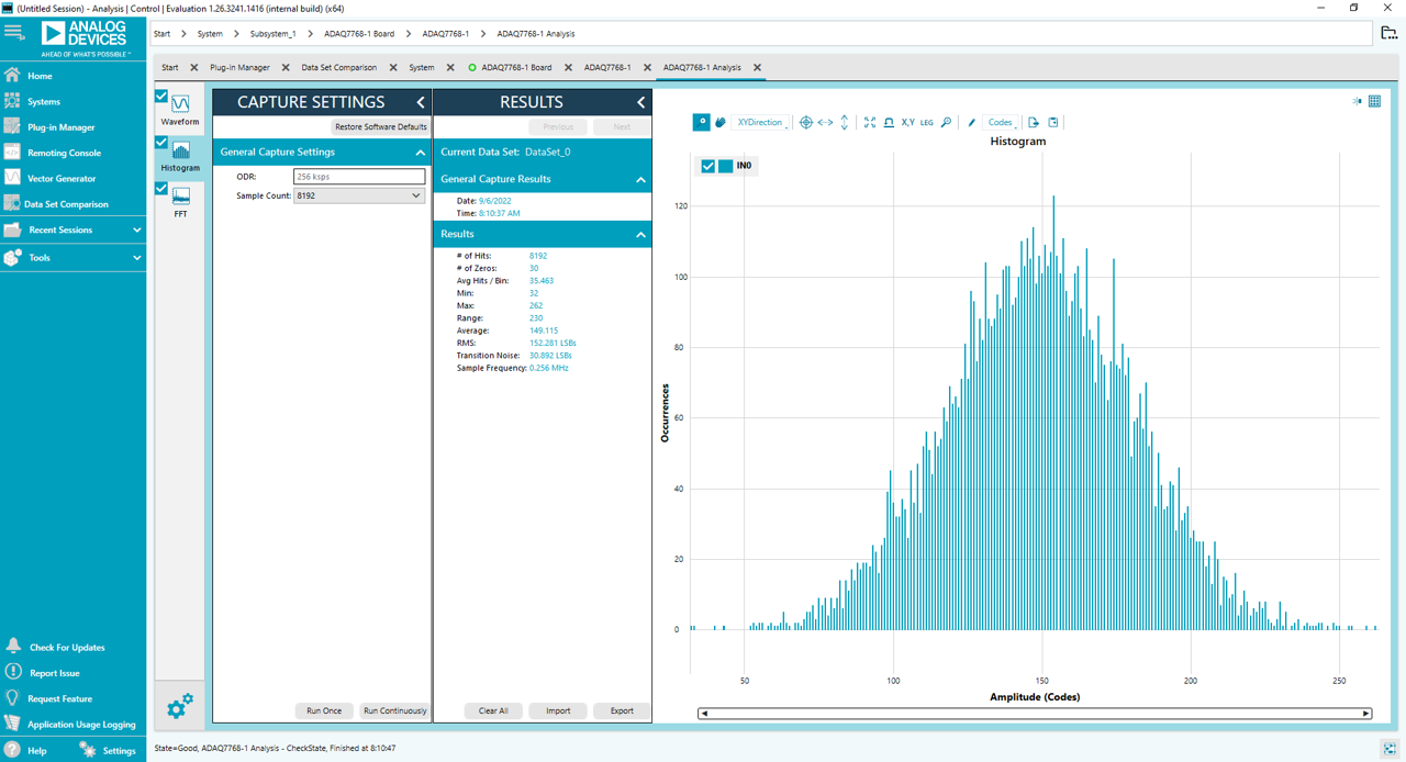
Histogram Tab
The Histogram tab contains the histogram graph, together with the capture results related to the DC performance (as shown in Figure 16).
The histogram graph displays the number of hits per code within the sampled data. This graph is useful for DC analysis and indicates the noise performance of the device.
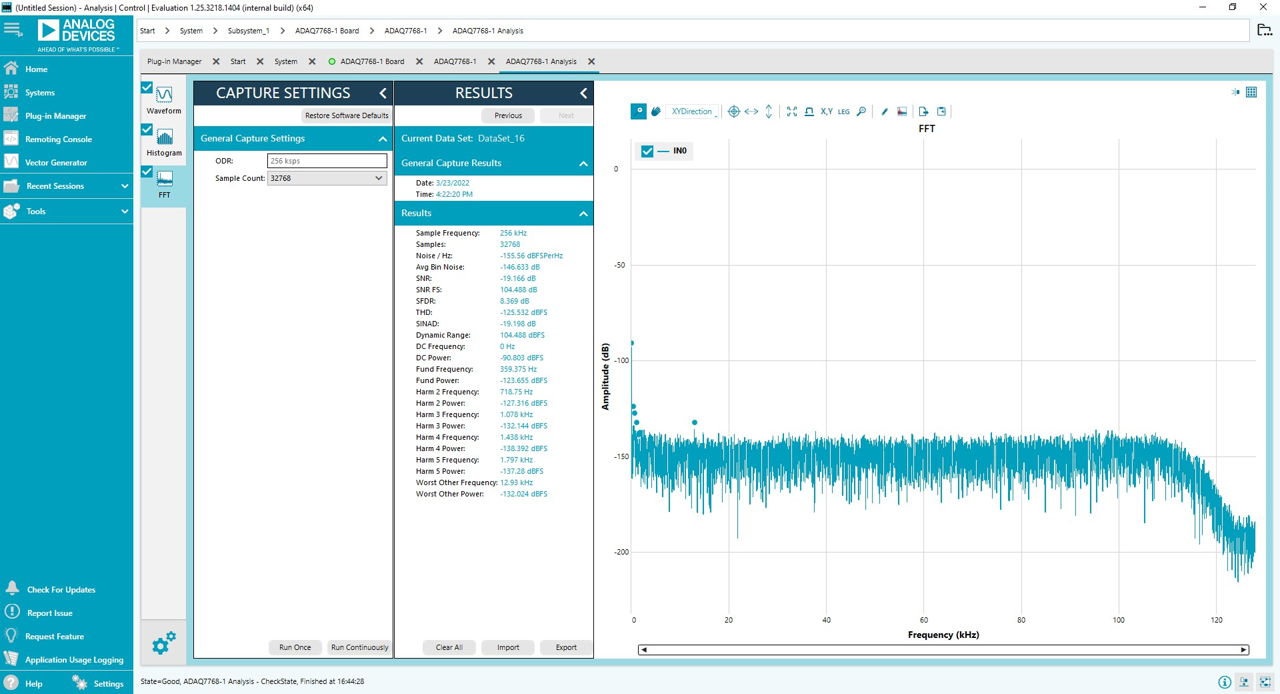
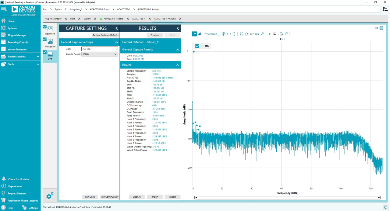
FFT Tab
The FFT results displays fast Fourier transform (FFT) information of the last batch of samples gathered, as shown in Figure 17.
The Signal section displays the fundamental frequency, and fundamental power. The Noise section displays the signal-to-noise ratio (SNR) and other noise performance results.
The Distortion section displays the harmonic content of the sampled signal, and the DC section displays the DC Power when viewing the FFT analysis.

Exiting the Software
To exit the software, click file icon on the upper right tab and then click Exit.
Configuring the Board
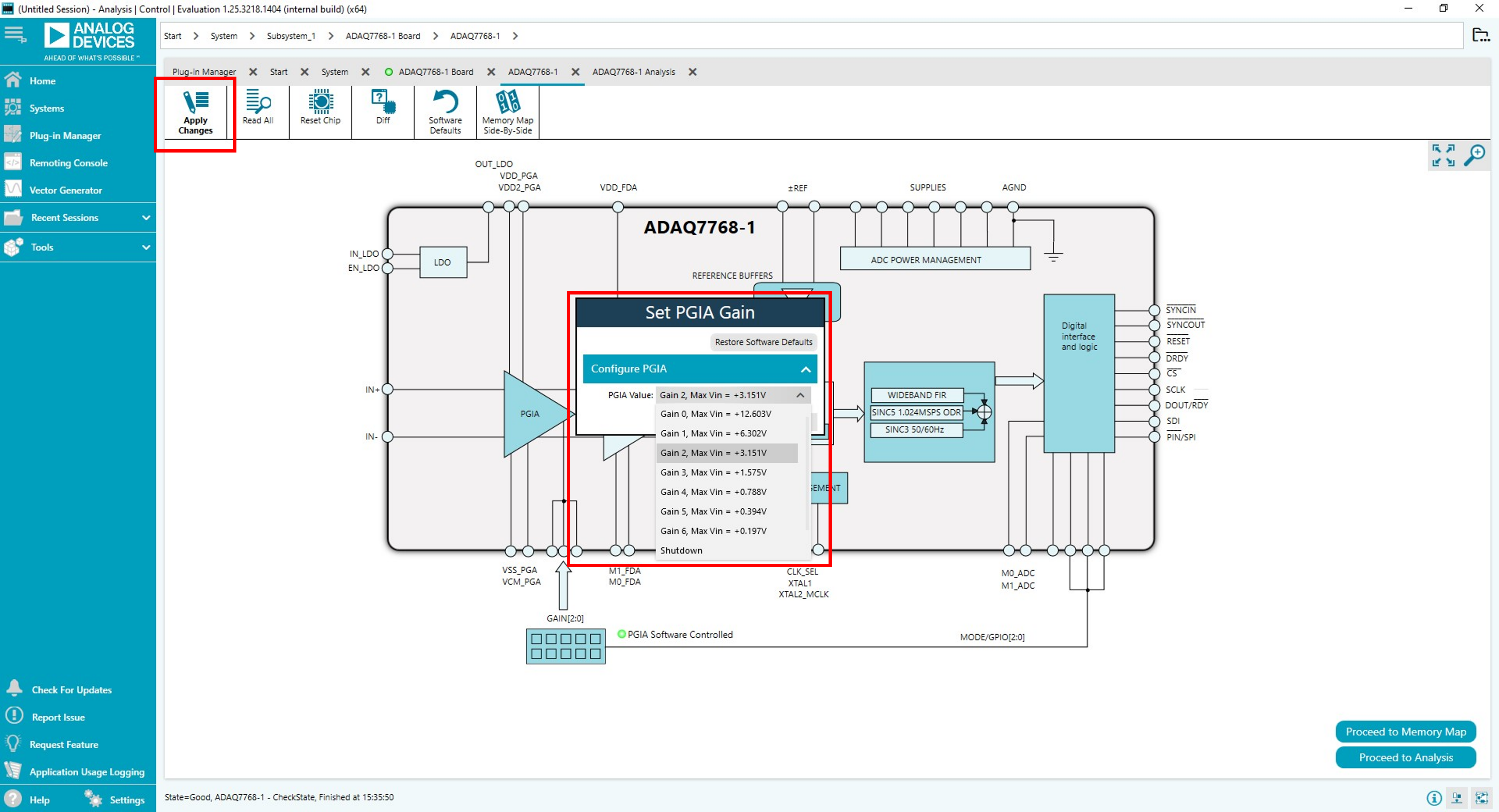
Input Range Control
There are two ways to control the DUT input range.
Through the GPIO of the DUT, controlled over the SPI interface.
Through on-board mechanical switch S2.
By default, the ACE software uses the GPIO to control the input range. The user can configure the PGIA gain by clicking the PGIA icon in the Chip View of the ACE software to select the input ranges. Once done, the user must click Apply Changes located at the upper left corner in order for the PGIA gain to take effect.
The user needs to set S2 switches to LO in order to properly control the device input range using GPIO.
Alternatively, the user can choose to select the input range through an onboard mechanical switch S2. For this to work, check the Control PGIA with switch in the PGIA Gain section. Then, click the Apply Changes for this to take effect.
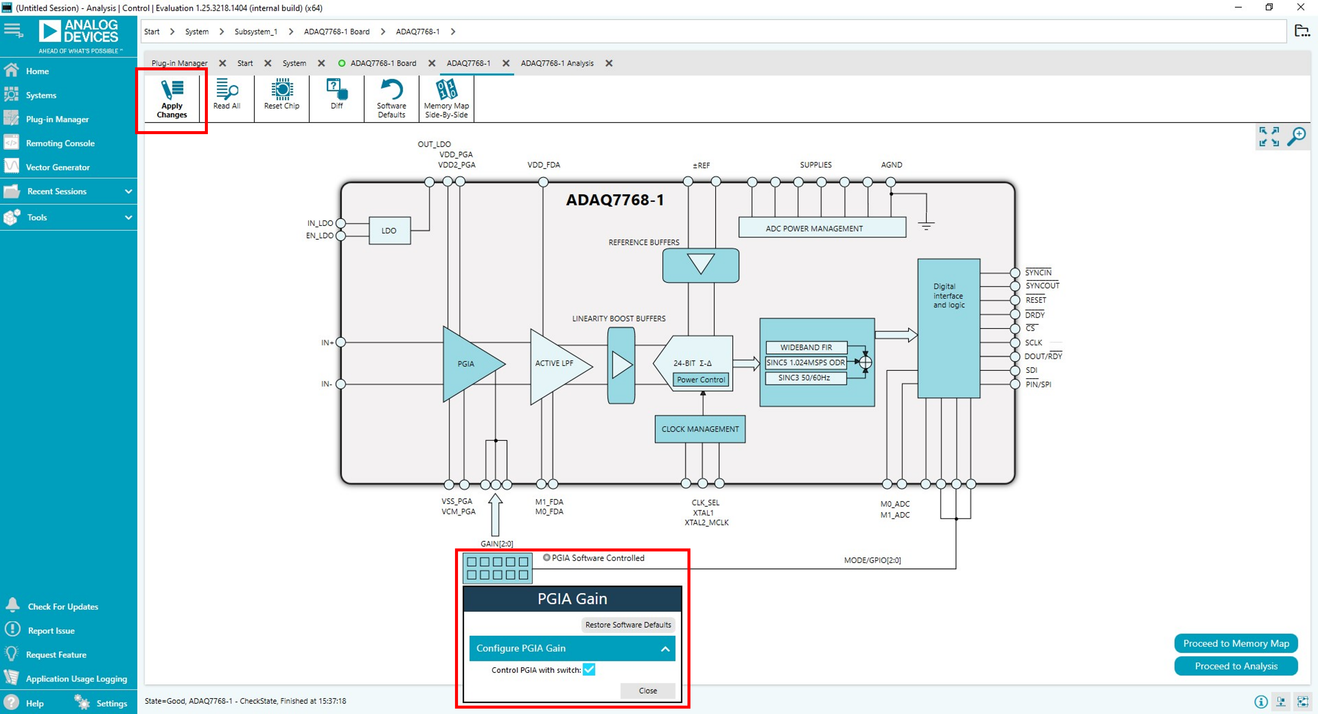
The user can then control the input range setting using switch S2, see Table 3 for more details. Note, when choosing the manual input range control option, the user is responsible for adjusting the Gain Mode Setting in the software accordingly in order for the software to display the correct measurement result.
Table 3. Configuration Switch S2 Functions
Name |
Description |
|---|---|
GAIN0, |
Gain mode/input range control for the ADAQ7768-1. |
GAIN1, |
(See Table 4 for more details.) |
GAIN2 |
Set to LO for GPIO input control mode. |
(labelled as |
|
A0, A1, A2 on |
|
Rev. A board) |
|
FDA_M0 |
Reserved. Default low. |
FDA_M1 |
Reserved. Default low. |
Table 4. PGIA Mode Settings
Gain Setting |
Differential Input Range (V) |
GAIN2 |
GAIN1 |
GAIN0 |
|---|---|---|---|---|
Shut Down |
H |
H |
H |
|
Gain0 |
±12.603 |
H |
H |
L |
Gain1 |
±6.302 |
H |
L |
H |
Gain2 |
±3.151 |
H |
L |
L |
Gain3 |
±1.575 |
L |
H |
H |
Gain4 |
±0.788 |
L |
H |
L |
Gain5 |
±0.394 |
L |
L |
H |
Gain6 |
±0.197 |
L |
L |
L |
Input Configuration
Provide the input signal through screw terminal or the SMB connectors.
The default board inputs are floating with high impedance. The user needs to ensure the source signal is properly biased to a common mode voltage.
The true dynamic range of the board can be measured by connecting the two inputs to the board’s ground reference through the screw terminal by a short piece of wire.
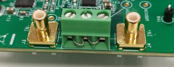
Figure 21 Short the inputs to ground with wire to measure the signal chain dynamic range
Configuring the DUT
The default configuration sets the DUT with the wideband low ripple (brick wall) filter with ODR=256ksps. The user can see the result by clicking Proceed to Analysis > Run Once button in the Chip View of the software.
Refer to the ADAQ7768-1 datasheet for more information on the DUT register configuration.
The ADAQ7768-1 has excellent performance in both AC and DC measurement. The digital filter inside the ADAQ7768-1 can be programmed with a wide range of decimation ratios to achieve input bandwidth from a few Hertz to a maximum of 204kHz.
AC Measurement
By default, the software configures the DUT to perform wide bandwidth measurement with the wideband low ripple digital filter (brick wall) of 110kHz of -3dB BW.
In this mode the user can evaluate the wide band dynamic range (noise) as well as other AC performances such as SNR, THD and SFDR etc.
The user can also test the device’s anti-aliasing performance by sweeping an out of band signal to the input across frequency.
DC Measurement
A Sinc3 filter with ODR=50SPS is a sweet spot for the measurement of a pure DC signal. As the Sinc notch appears at 50Hz and can be used to reject the 50Hz line frequency. Take the following steps to setup the DUT for a 50SPS Sinc3 filter:
As an example for RMS noise, short IN- and IN+ connectors to ground.
At the Chip View of the ACE software, click the Filter Configuration icon.
Use the drop-down menu to select Sinc3 (programmable decimation rate) option as shown in Figure 23.
Configure the Sinc3 Decimation Rate by typing in the value ‘13FF’ in the text box near the lower right corner as shown in Figure 24. This is also reflected in the registers SINC3_DEC_RATE_LSB and SINC3_DEC_RATE_MSB located at the memory map of the ACE software (see Figure 25). Afterwards, click Apply Changes for this to take effect.
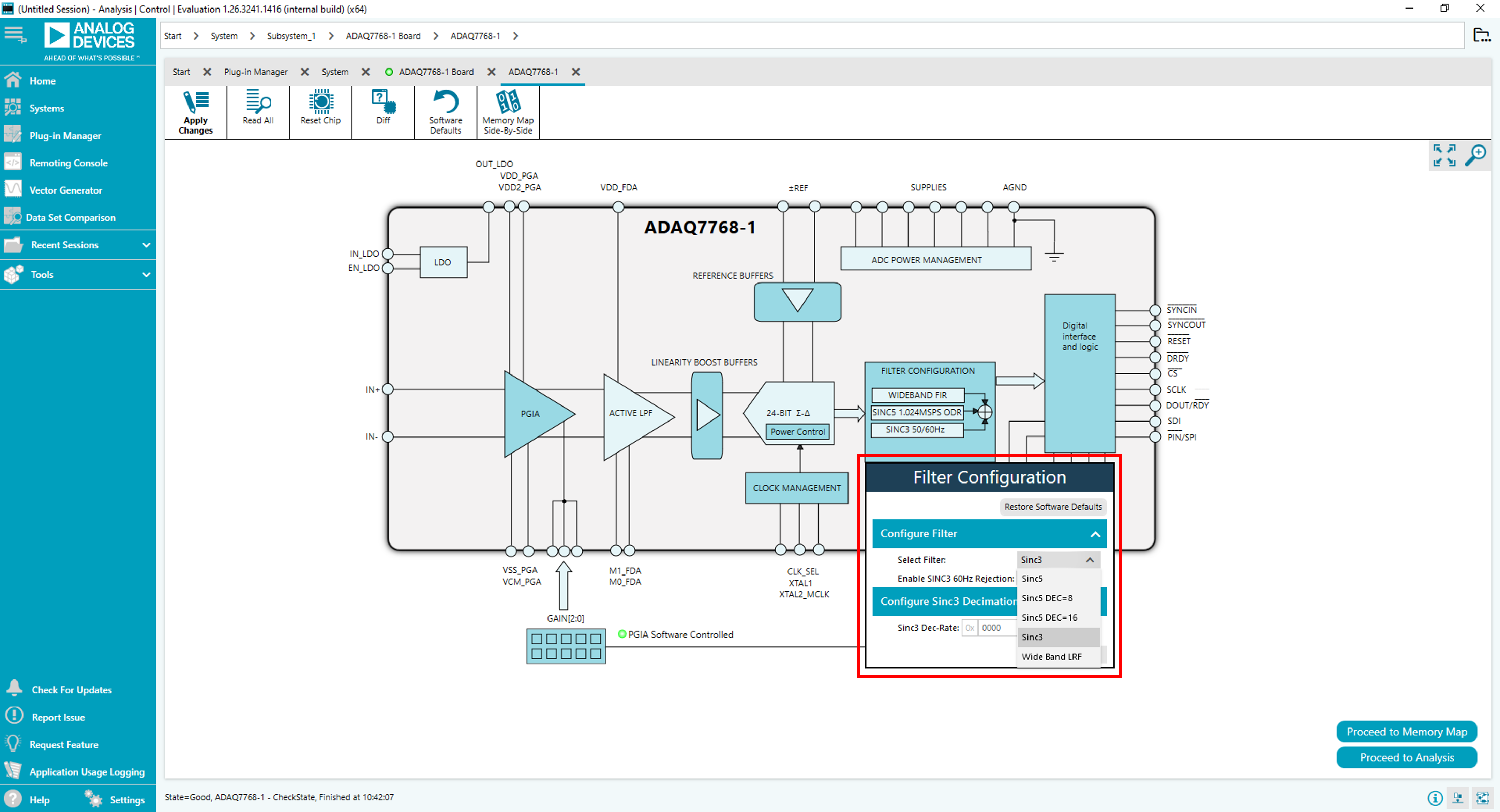
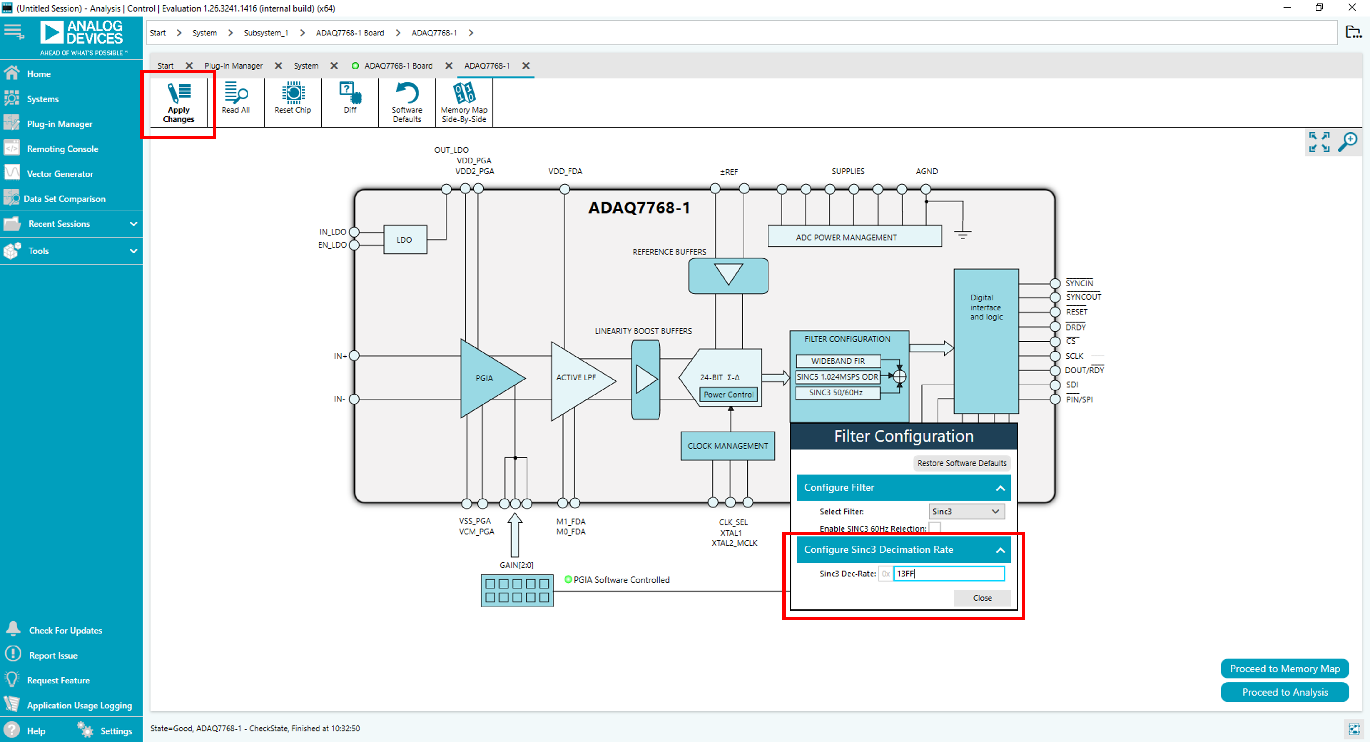
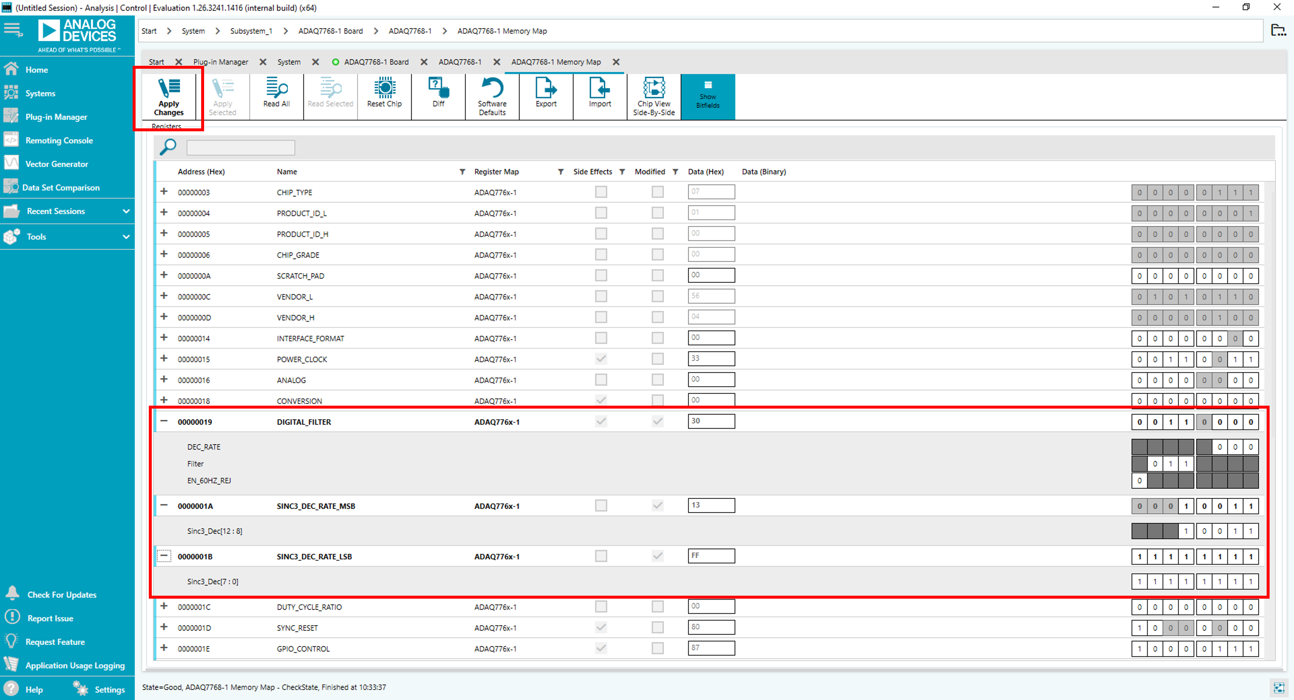
Figure 25 Sinc3 filter decimation ratio using Memory Map View.
Before clicking on the Run Once button, make sure to adjust the number of samples to be collected accordingly.
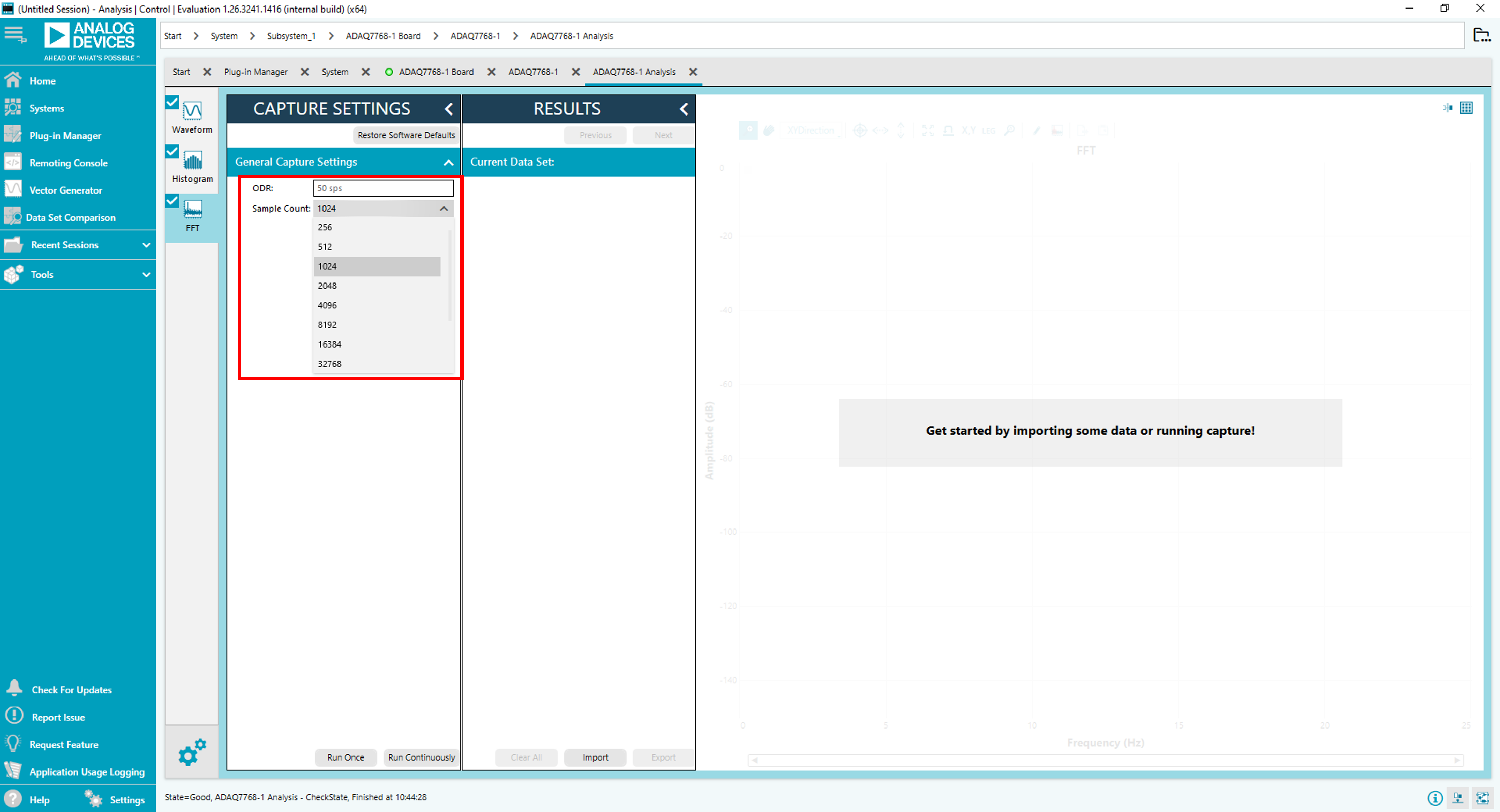
Figure 26 Change the number of samples to collect per sample run
Collecting the default 8192 samples at 50SPS will take 8192*1/50/60=2.73 minutes! Start with 1024 samples, which should take about 20 seconds. Generate new capture using 1024 samples.
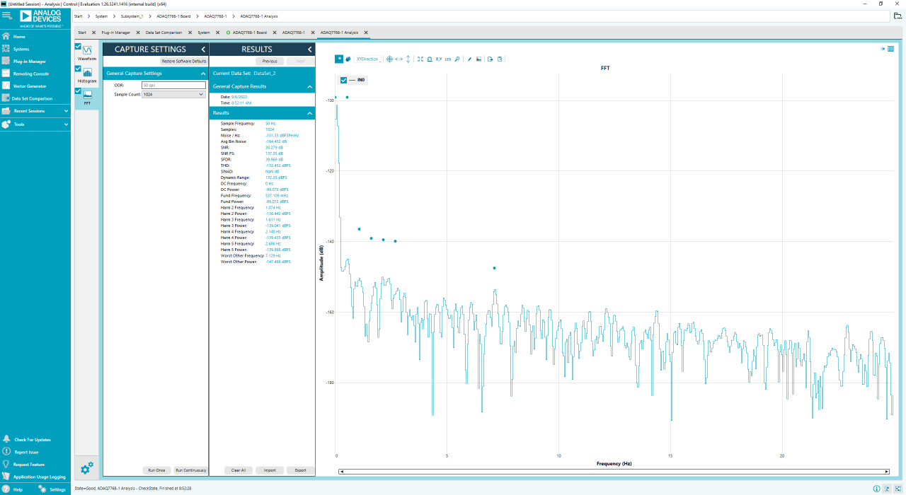
Figure 27 FFT plot for a typical DC measurement, with Gain6 mode, input shorted, ODR=50sps, 1024 samples.
The same condition (Sinc3 50SPS) is used to measure Low Frequency Noise, as specified in the datasheet. In the Histogram tab, noise is displayed as Transition noise in LSB. To compare with datasheet’s referred to input (RTI) Low Frequency Noise in μVrms, apply the formula:
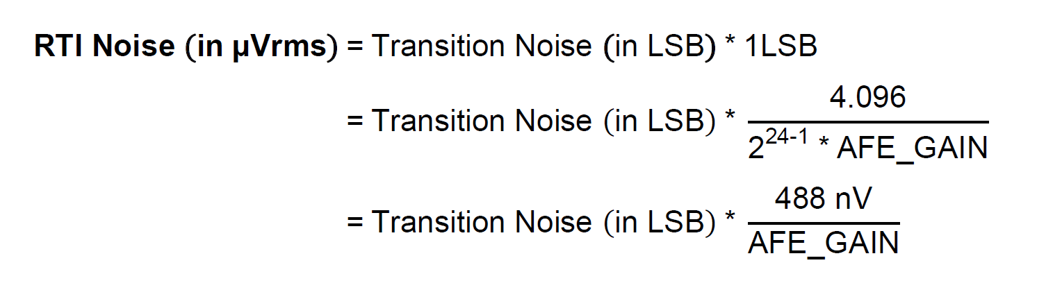
For example, using Gain2 Mode (AFE_GAIN = 1.3 V/V) with measured Transition Noise = 1.508 LSB = 0.566 μVrms RTI.
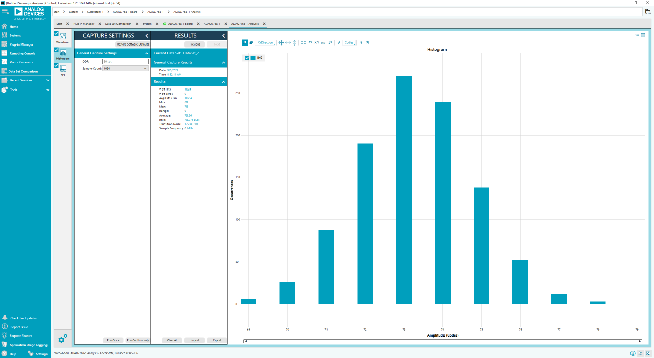
Figure 28 Histogram of output codes. with Gain2 mode, input shorted, ODR=50sps, 1024 samples.
Calculating SINC3_DEC_RATE Value
For a 16.384 MHz MCLK to achieve an ODR of 50 Hz using the Sinc3 filter, use the following equation and determine the DEC_RATE:
\(ODR = Mclk/MclkDiv \times DecRate\)
With the ADAQ7768-1 MCLK_DIV = 2,
\(DecRate = Mclk/MclkDiv \times ODR = 163,840\)
To program the Sinc3 decimation ratio, the user must first calculate for the equivalent Sinc3 decimation ratio to be written on SINC3_DECIMATION_RATE registers (SINC3_DEC_RATE_MSB and SINC3_DEC_RATE_LSB) using the equation below:
\(Equivalent DecRate = DecRate/32 -1 = 5119\)
To set the decimation ratio to 163,840, write the equivalent hexadecimal value of 5119 to SINC3_DEC_RATE_MSB and SINC3_DEC_RATE_LSB registers because the value in the register is incremented by 1 and then multiplied by 32 to give the actual decimation rate.
Refer to the ADAQ7768-1 datasheet for more information on the DUT register configuration.
Reset Switches
Press S1 switch to reset the DUT. Resetting the DUT will reset all the register settings to its default value.
A reset switch is also available on the SDP-H1 to reset the interface board. Resetting the digital interface board will result in losing communication with the DUT.
The user can restart the software tool to re-initialize the board.
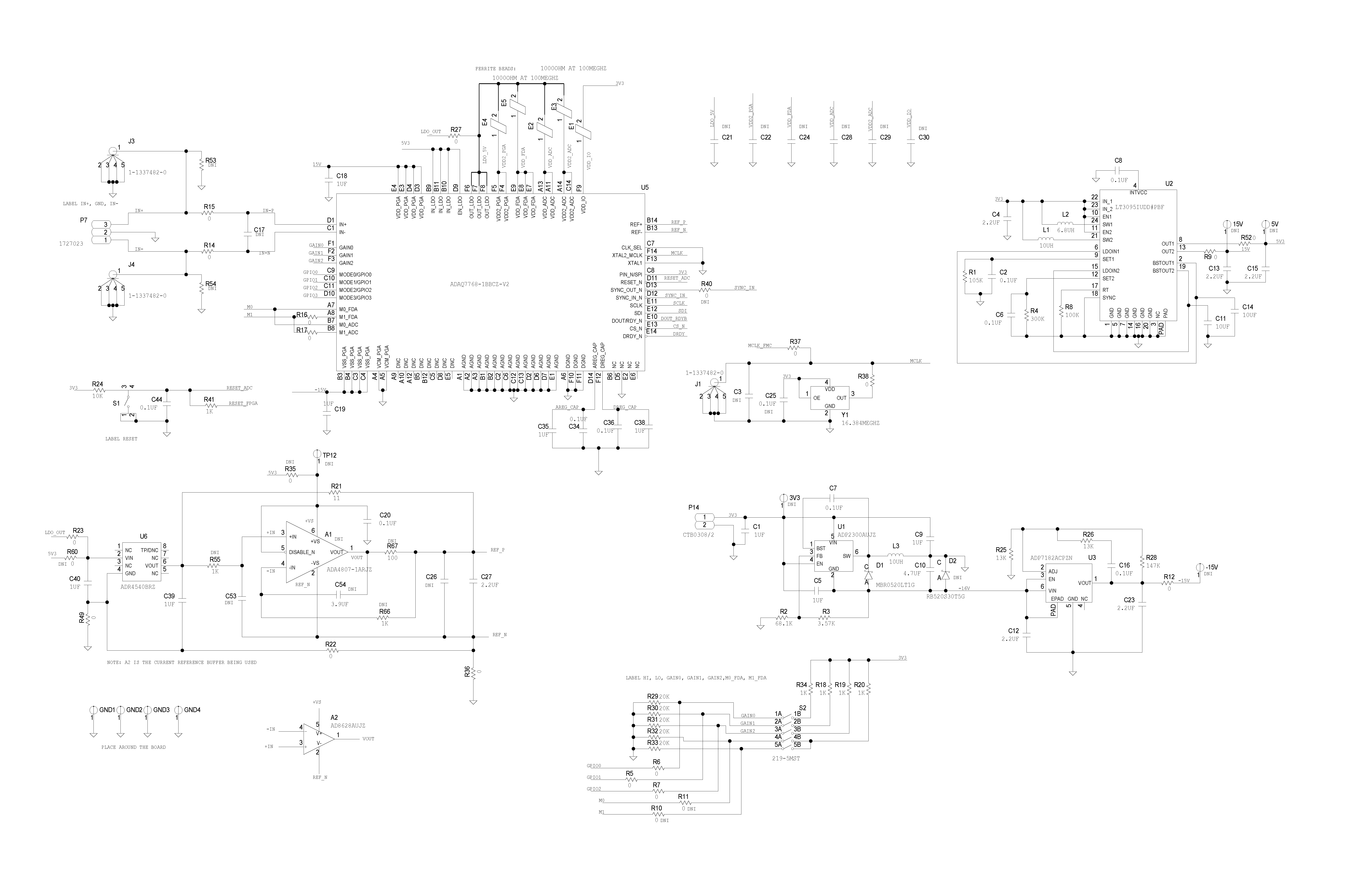
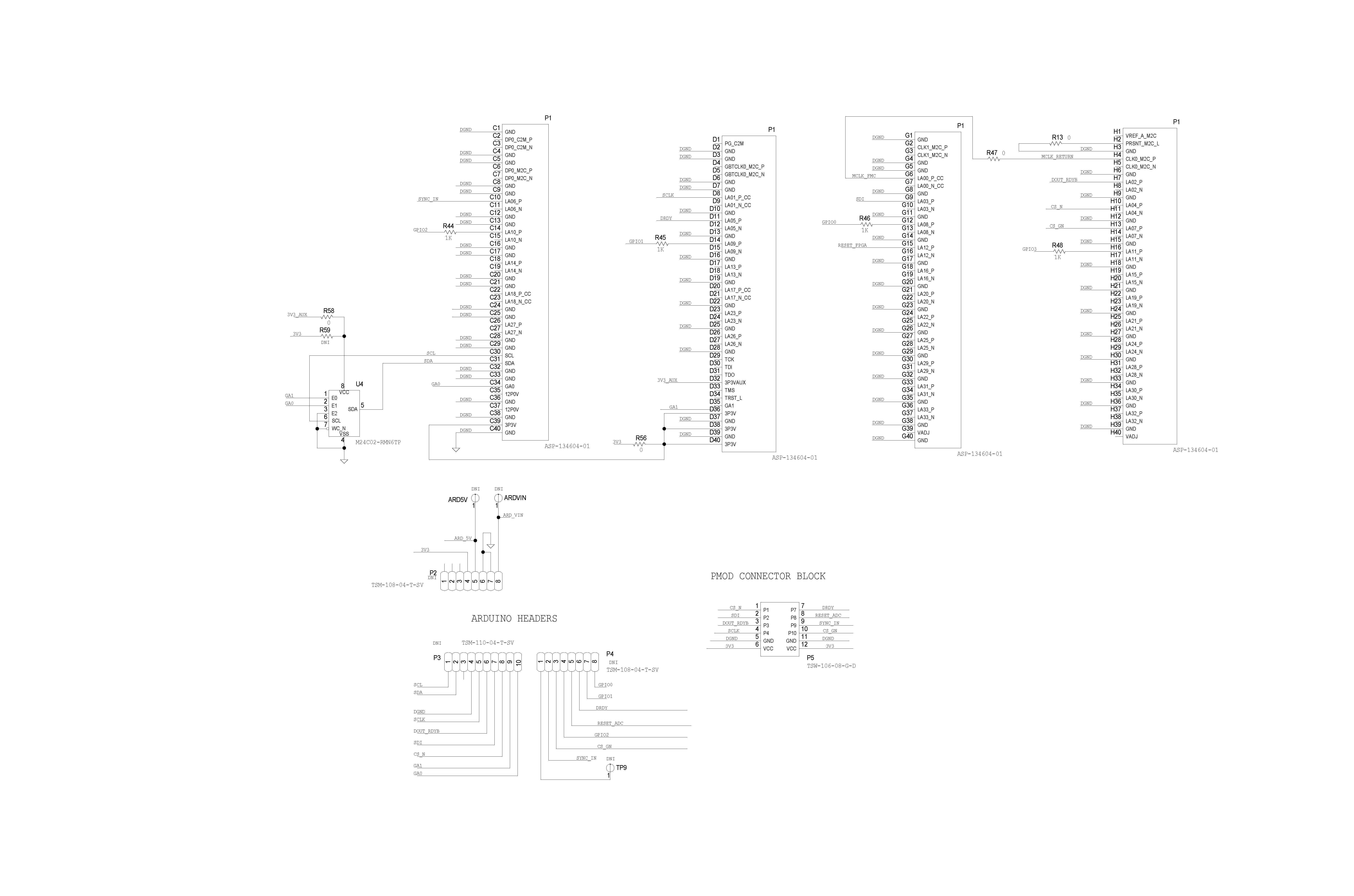
Evaluation Board Schematic