AD-FMCDAQ3-EBZ (Rev C) Functional Overview
The system consists of four functional partitions - transmit path, receive path, clocking and power supply. A functional block diagram of the system’s main components and signal paths is given below. The power tree and voltage monitoring are included in the Power section below.
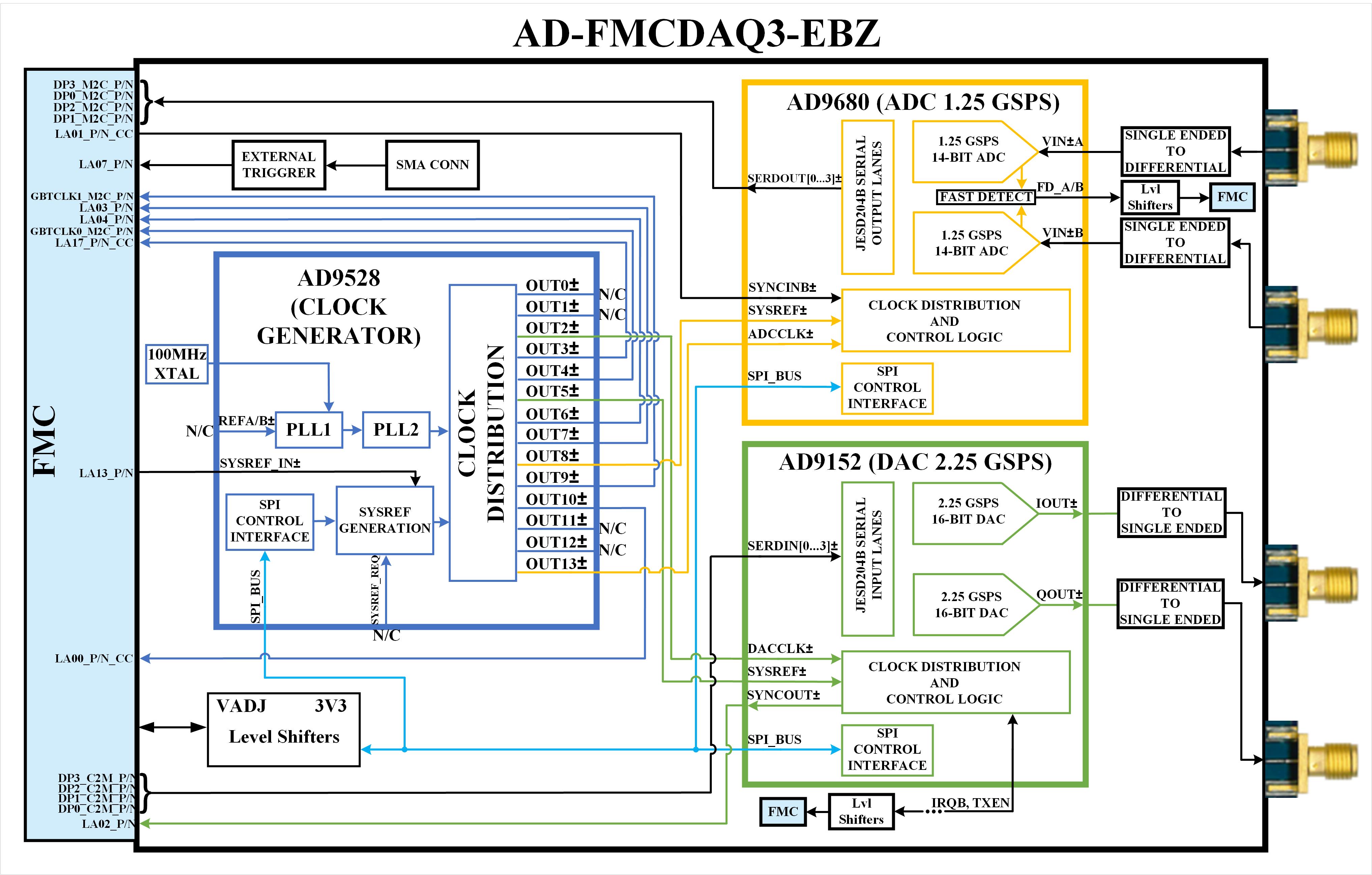
Transmit
Key component:
Dual, 16-Bit, 2500 MSPS, TxDAC+® Digital-to-Analog JESD204B Converter with offset, phase and gain compensation. |
The reference design generates the signals for AD9152 either from an internal DDS or external memory (via VDMA). The internal DDS consists of four independent signal generators with programmable phase offset and frequency. These four signal generators are paired to create two tones that are interleaved and driven to the DAC.
Receive
Key component:
14-Bit, 1250 MSPS, Dual Analog-to-Digital JESD204B Converter (ADC). |
The reference design transfers the received data to DDR via DMA. An optional off-line FFT core may be used to generate a spectrum plot.
Clocking
Key component:
Low Jitter Clock Generator (1MHz to 1.25GHz) with 14 Outputs. |
The system is clocked through an on board crystal (100MHz). The clock path mainly consists the AD9528 which up converts this signal to ~3.7GHz, and then divides this back down to any integer divider of this ~3.7GHz output.
The default reference design that ADI provides does the following:
Crystal generates a fixed clock frequency of 100MHz.
This clock is sent to the AD9528.
The AD9528 takes this, and creates:
1233 MHz for the DAC sample rate
1233 MHz for the ADC sample rate
616 MHz for the reference clocks to FPGA
These clocks can be changed, but the key thing to remember is that the AD9528 drives both the ADC and DAC. The AD9528 has various clock banks. The best thing to do if you are interested in the details of this, is to get the Eval board software, and play with the different settings (you don’t need a demo board connected to run the software).
Power
The system-level power tree .ltp3 file simulated in LTpowerPlanner is given below. 220309_fmcdaq3_power.zip
Key components in the power tree:
4A, 20V step-down switcher. |
|
High accuracy, 500mA LDO |
|
Ultra low noise, 150/200 mA LDO |
|
Low VIN, 2A LDO |
|
Low VIN, 1.2A LDO |
|
Low VIN, 600mA LDO |
The board receives all the power from the FPGA board through FMC.
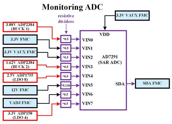
The monitoring function of board’s DC voltages is accomplished using AD7291 SAR ADC. The block diagram of the ADC and the corresponding monitored voltages is shown below.
VADJ pin from FMC connector is used for supplying the translators VCCA voltage. Supported voltage values of this pin are: 1.2V/1.5V/1.8V/2.5V/3.3V.
For differential to single-ended conversion and for minimizing 2nd harmonic distortion in transmitting and receiving, a double-balun configuration is used for TX and RX as front-end interface. More topology detail and information about the front-end design insights are presented in the following articles: