Quick Start Guide for Testing the AD9213 Customer Evaluation Board AD9213-10GEBZ-B Using the ADS8-V1EBZ FPGA-Based Capture Board
Typical Setup
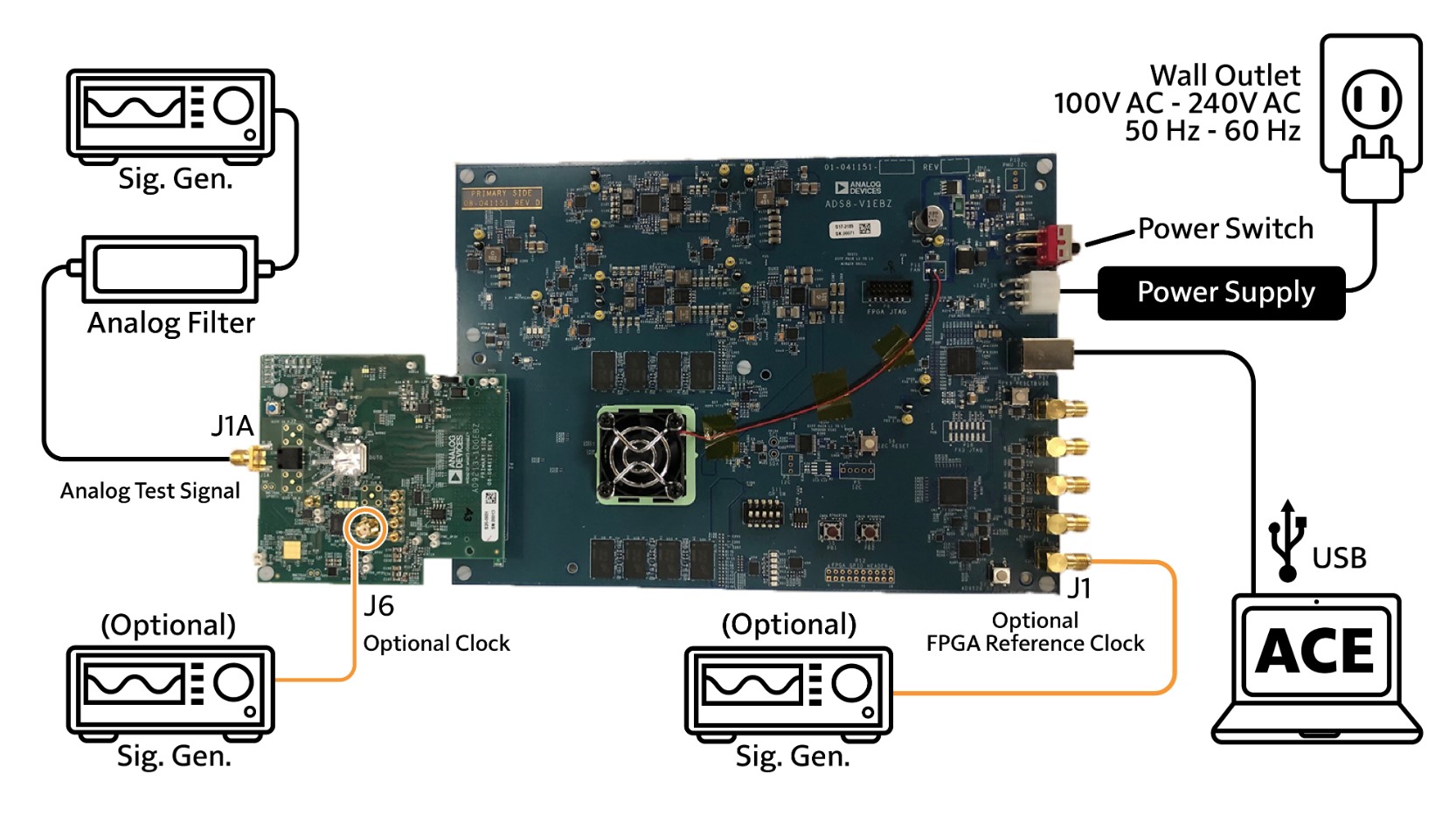
Figure 1 AD9213-10GEBZ-B Evaluation Board and ADS8-V1EBZ Data Capture Board, default configuration with external clocks.
Configuration for External Clocks
The AD9213 is able to be configured for on-board clocking or external clocking.
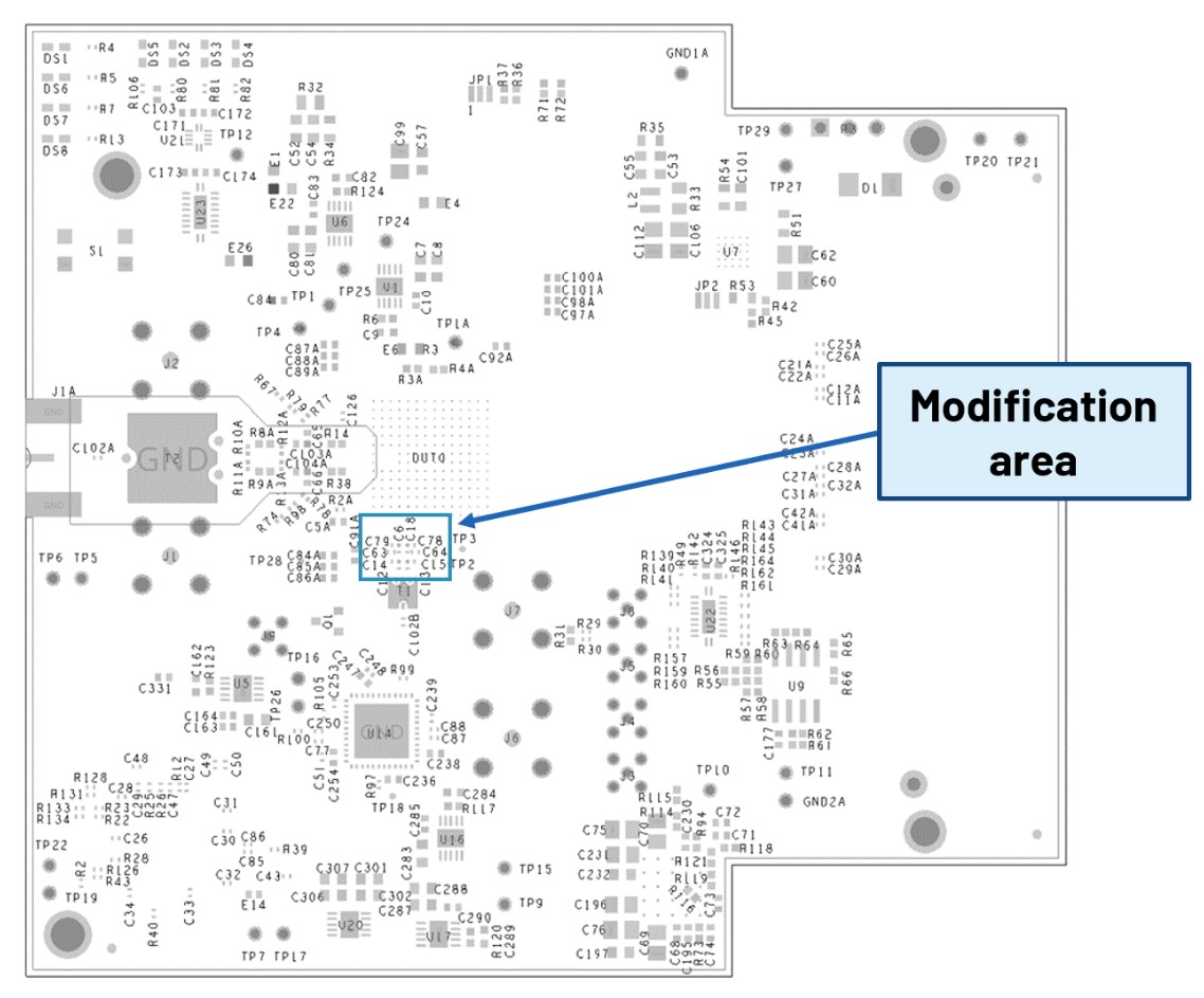
To alter an on-board clocking AD9213 evaluation board to be used for external clocking, capacitors C78 and C79 need to be removed, and C6 and C18 need to be placed. The figure below displays where these capacitors are located on the board
The figure below displays a zoomed in view of the clocking capacitors. Please note that the capacitors outlined in orange, C78 and C79 are for on-board clocking, and the capacitors outlined in blue, C6 and C18, are for external clocking. In addition, although these capacitors are all the same package size, note that the on-board clocking capacitors are 1nF capacitors, and the on-board clocking capacitors are 10nF capacitors.
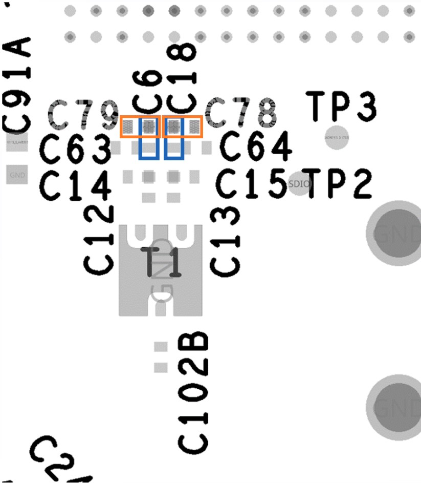
Please refer to the Board Design and Integration Files for more information about the sizing and values of components.
See the steps below in Equipment Needed to set up the two (otherwise optional) signal generators necessary for external clocking AD9213 evaluation board.
Equipment Needed
Signal Generators
Analog signal source: The frequency and power requirements depend on the tests to be performed. A bandpass filter is typically used for single tone tests.
Optional sample clock source: The AD9213-10GEBZ-B, AD9213-6GEBZ-B, AD9217-10GEBZ-B and AD9217-6GEBZ-B are equipped with on-board sample clock generation capability, so an external clock source is not needed. If an external sample clock source is desired, the clock signal generator should have very low phase-noise and be capable of supplying a 10Ghz clock signal (or 6 GHz clock signal for the the 6Gsps speed grade of AD9213/AD9217) at approximately 10dBm.
Optional FPGA Reference clock source: The AD9213-10GEBZ-B, AD9213-6GEBZ-B, AD9217-10GEBZ-B and AD9217-6GEBZ-B are equipped with on-board FPGA reference clock generation capability, so an external FPGA reference clock source is not needed. If an external sample clock source is desired, for AD9213-10GEBZ-B with 16 output lanes (at 10Gsps), the frequency of REFCLK is 625MHz. For AD9213-6GEBZ-B configured for 8 output lanes (at 6Gsps), the frequency of REFCLK is 750MHz. For AD9213, the frequency of REFCLK is the digital output lane rate divided by 20. For AD9217, the frequency of REFCLK is the sample rate divided by 16, which is the same as digital output data rate divided by 16.
PC running Windows®
USB port and cable to connect to a PC
AD9213/9217 Evaluation Board
ADS8-V1EBZ FPGA Based Data Capture Board with a power supply
Helpful Documents
AD9213 Data Sheet
ACE Manual: http://swdownloads.analog.com/ACE/ACE_User_Manual_rev3.pdf
Software Needed
Analysis Control Evaluation (ACE) software: available at /en/resources/evaluation-hardware-and-software/evaluation-development-platforms/ace-software.html
Board Design and Integration Files
Description |
Download |
|---|---|
AD9213-10GEBZ-B Schematics |
|
AD9213 Evaluation Board BOM and Layout Files |
|
Bill of Materials for on-board clocking AD9213 |
|
Gerber Layout files for on-board clocking AD9213 |
Testing
Install the ACE software. The installer is located at https://swdownloads.analog.com/ACE/ACEInstall_1.30.3369.1491.exe. The Start page appears after you complete the installation and open ACE. The Start page displays released plugins. Ensure that the AD9213/9217 plugin appears in the pre-installed list of released plugins.
If the AD9213/9217 plugin does not appear in the pre-installed list, it is also available here: en/design-center/evaluation-hardware-and-software/evaluation-boards-kits/EVAL-AD9213.html#eb-relatedsoftware
Close ACE.
Install jumper on P3 as shown below.
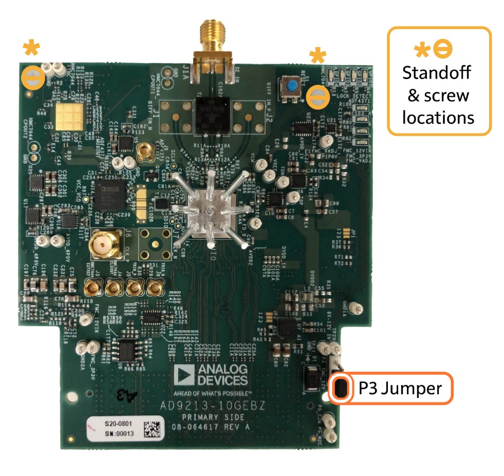
You can install standoffs at the locations (marked with an *) if needed. Alternatively, you can use foam sheets to support the board.
Connect the AD9213/9217 evaluation board to the ADS8-V1EBZ board together as shown in the following figure.
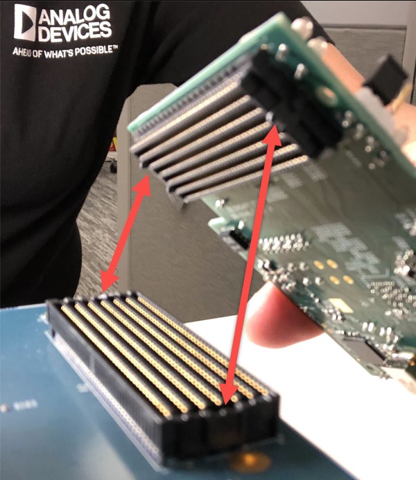
Align the FMC+ connectors and apply even pressure across the connector and press the FMC connector on to its counterpart on the FPGA board.
Connect signal, clocks (optional), power and USB cables to the boards as shown in Figure 1.
Signal (J1A): The frequency and amplitude of the test signal depend on the type of test you are performing. Full scale is typically achieved at 9dBm – 12dBm signal power at the signal generator (depending on the frequency, and insertion loss of the filter used). If in doubt about which amplitude to use, start with a lower amplitude (for example, 4dBm at the signal generator) and work up or down from there.
Optional Sample clock (J6): The sample clock works well across a wide range of amplitudes (1dBm – 10dBm at the signal generator). Because jitter performance is likely to improve as the slew rate increases, choose an amplitude towards the upper end of the stated range.
Optional FPGA Reference Clock (ADS8-V1EBZ J1): Similar to the sample clock, the reference clock works well across a wide range of amplitudes (1dBm – 10dBm at the signal generator). Unlike the sample clock, the reference clock is not sensitive to jitter/phase noise. Any signal generator that meets the frequency and power requirements works. For AD9213, the frequency of the reference clock is the (output digital data rate)/20. For AD9217, the frequency of the reference clock is the (output digital data rate)/16. The FPGA reference clock must be synchronized with the ADC sample clock.
Example: For the default JESD204B output configuration of AD9213-10GEBZ (L = 16, N’ = 16, M = 1) at 10Gsps, the output data rate is 12.5Gbps. Reference clock frequency =12.5G/20 = 625MHz.
Example: For AD9213-6GEBZ, ACE brings the part up in 8-Lane mode. In this case (L = 8, N’ = 16, M = 1) at 6Gsps, the output data rate is 15Gbps. Reference clock frequency = 15G/20 = 750MHz.
Connect the USB cable from the ADS8-V1EBZ FPGA board to the Windows PC that has ACE installed.
Power on the ADS8-V1EBZ FPGA board using the switch S4. Wait several seconds after powering on the ADS8-V1EBZ, until DS17 flashes and the FPGA fan has stopped spinning.
Start ACE from Start->Programs->Analog Devices->ACE.
ACE will auto-detect the AD9213 or AD9217 board and bring up the correct ACE plugin, which will appear in the upper left portion of the GUI. If the plugin does not appear in the upper left, select Plug-in Marketplace and select AD9213-10GEBZ-B, AD9213-6GEBZ-B, AD9217-10GEBZ-B or AD9217-6GEBZ-B, and add the selected plugin.
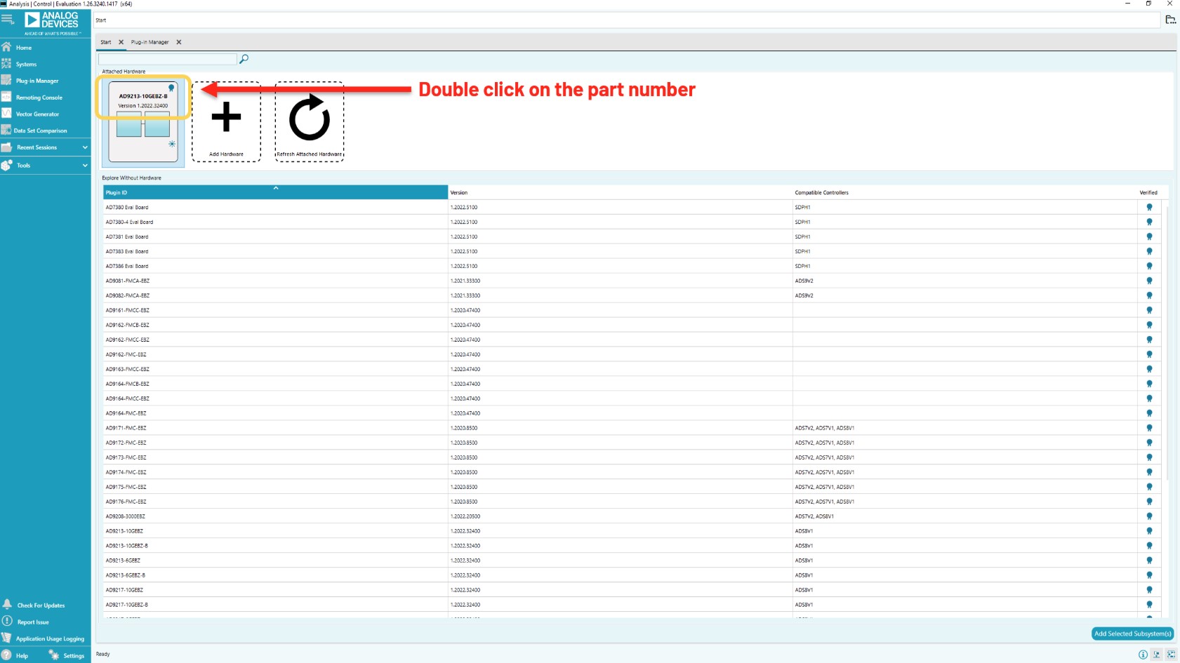
Double click on the AD9213 or AD9217 part number in the plugin icon in the upper left of the GUI.
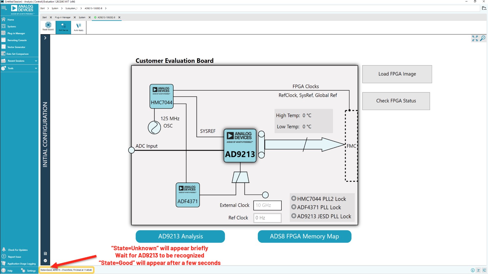
“Unknown” initially appears in the lower left corner. Wait until “Unknown” changes to “Good.”

After “State=Good” appears in the lower left, turn on the signal generators for the clock, reference clock, and signal.
Open the menu “Initial Configuration”.
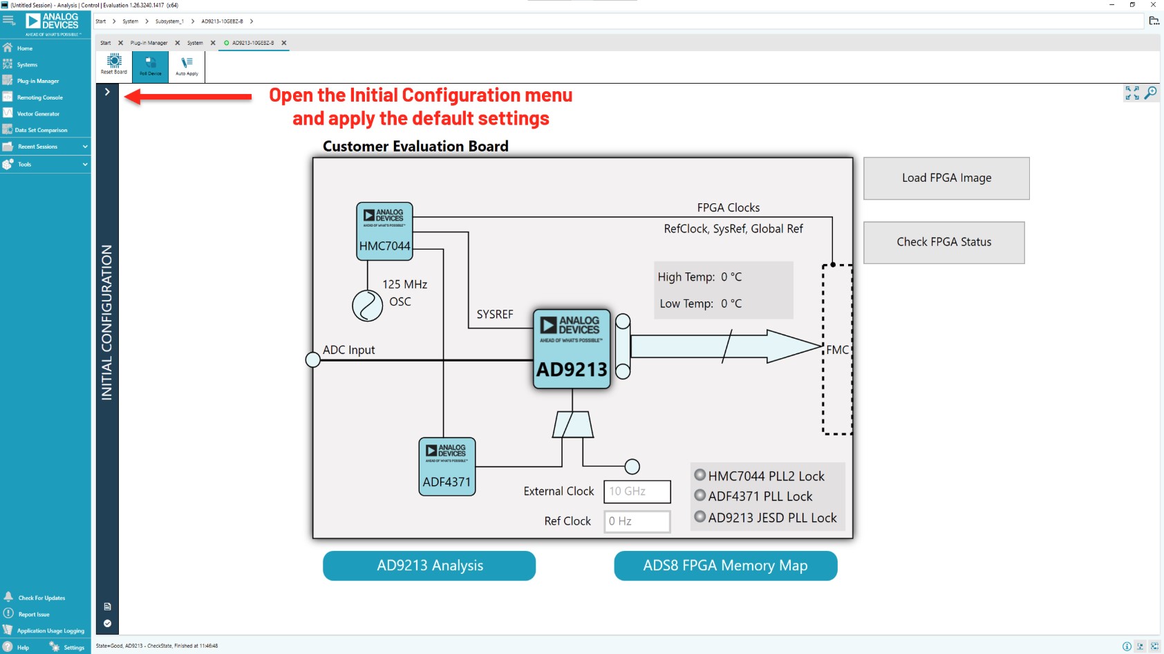
Figure 9 On-board clocking: Open the Initial Configuration menu to apply the default configuration settings.
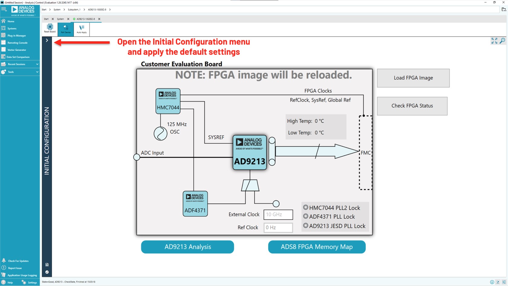
Figure 10 External clocking: Open the Initial Configuration menu to apply the default configuration settings.
Click the Apply button to configure AD9213 in its default full bandwidth mode configuration. Then double-click on the chip to proceed.
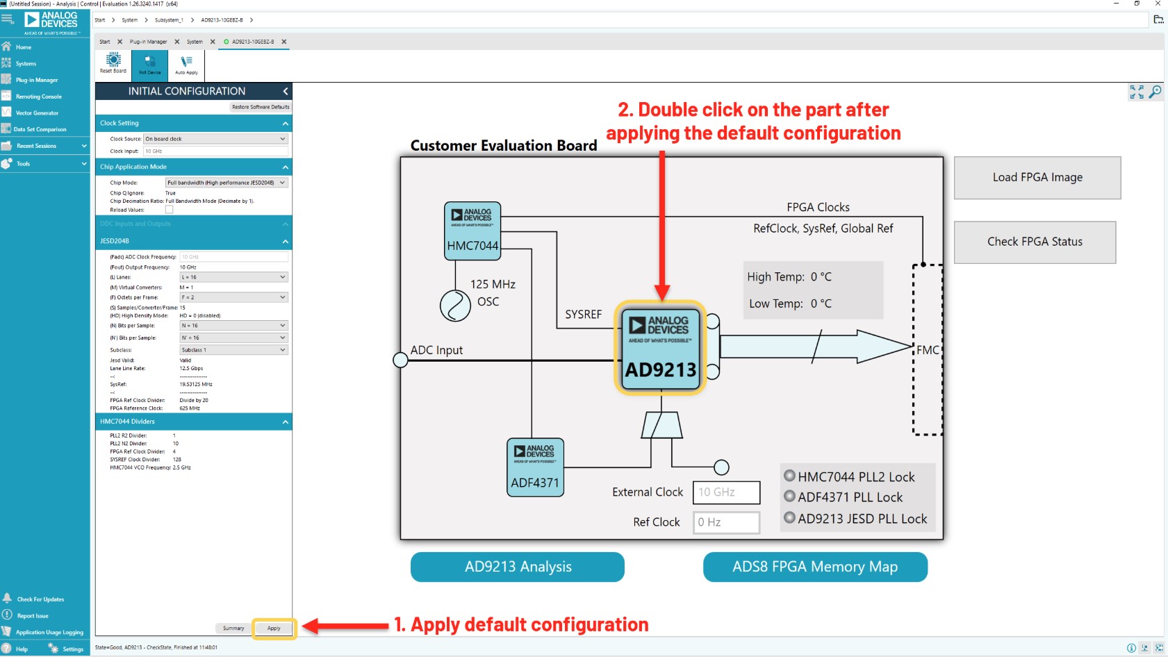
Figure 11 On-board clocking: Apply default settings in the Initial Configuration menu before double-clicking on the chip.
“Output Interface PLL Locked” will appear green. Confirm that “Common mode” is set to “Startup: Internal VCM Control” and then click “Proceed to Analysis
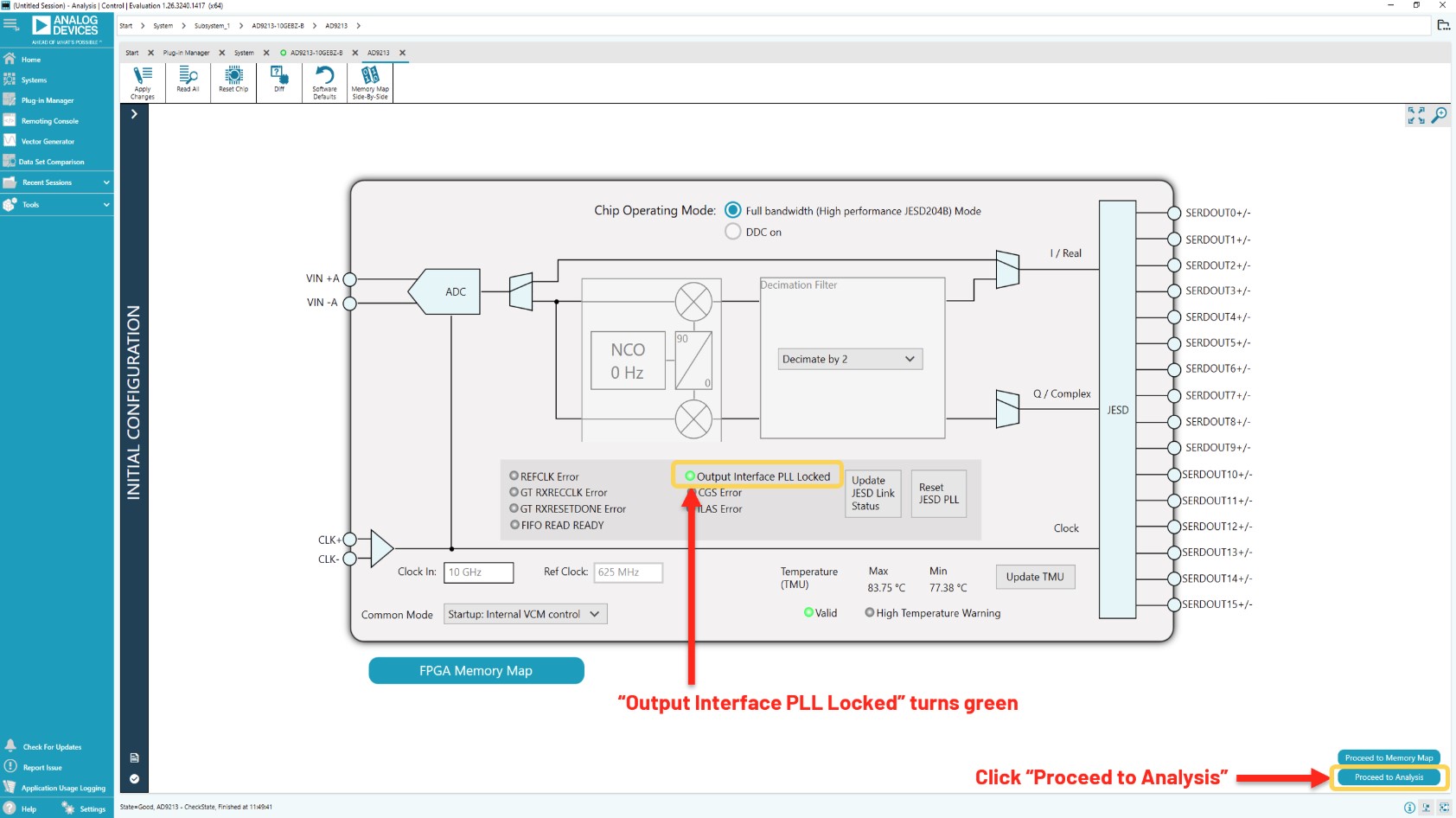
Figure 12 On-board clocking: Proceed to Analysis in full bandwidth mode
For DDC mode, please set the chip mode to “DDC on” and configure as necessary. Please note the ref clock frequency can change based on which modes are selected, and adjusting the frequency applied to the ADS8-V1EBZ may be necessary. After applying desired settings, click “apply”, and then double click on the part.
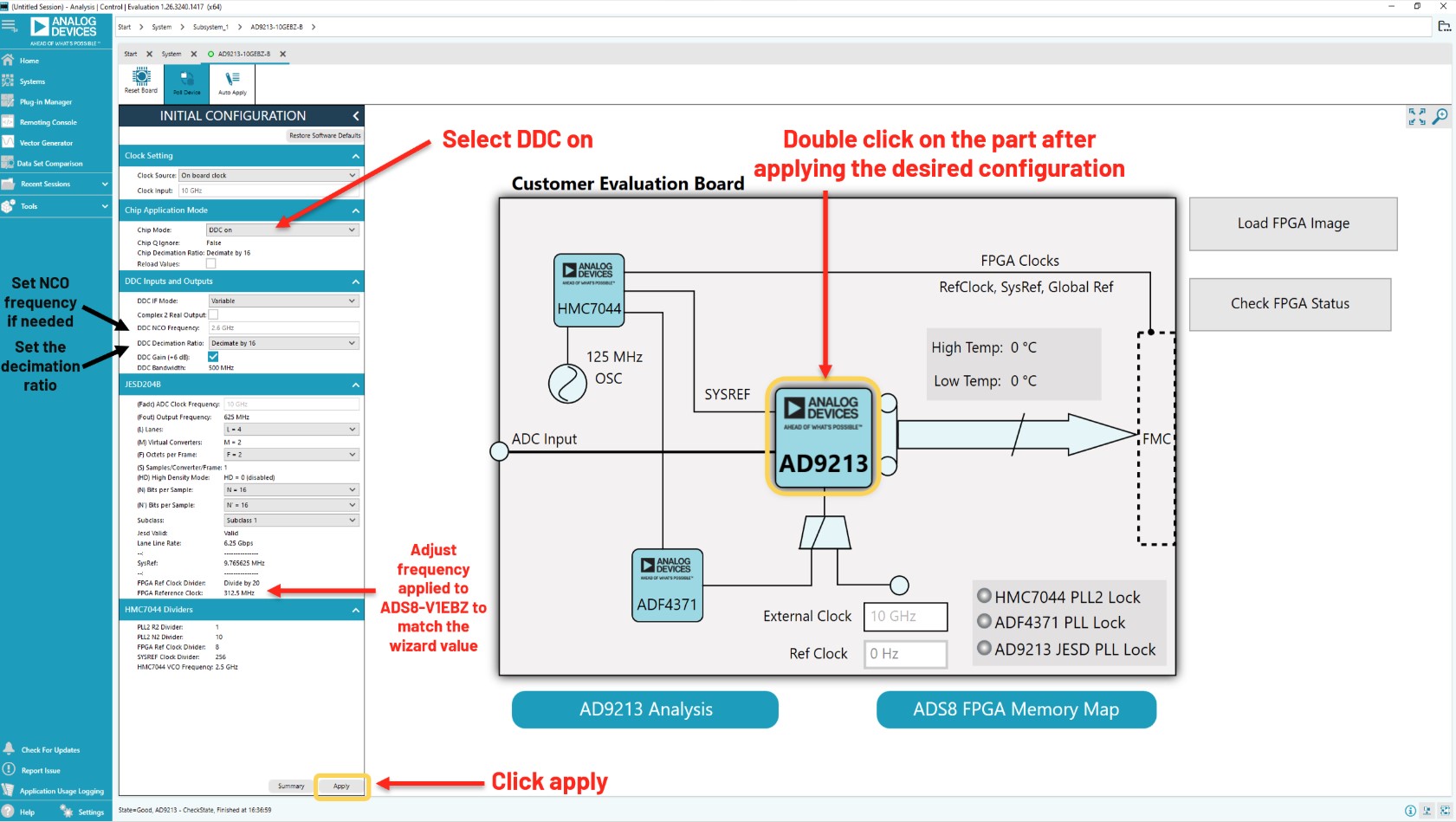
Figure 13 On-board clocking: Apply default settings in the Initial Configuration menu before double-clicking on the chip.
“Output Interface PLL Locked” will appear green. Confirm that ‘Common mode” is set to “Startup: Internal VCM Control” and then click “Proceed to Analysis
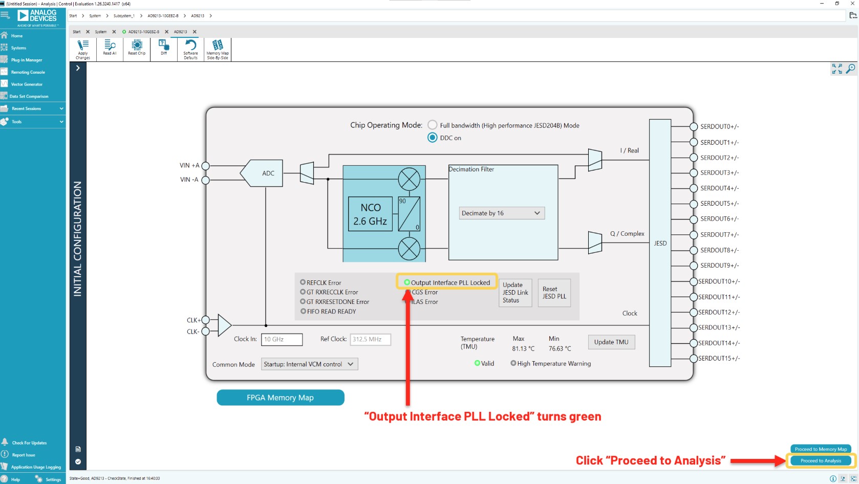
Figure 14 On-board clocking: Proceed to Analysis in DDC mode
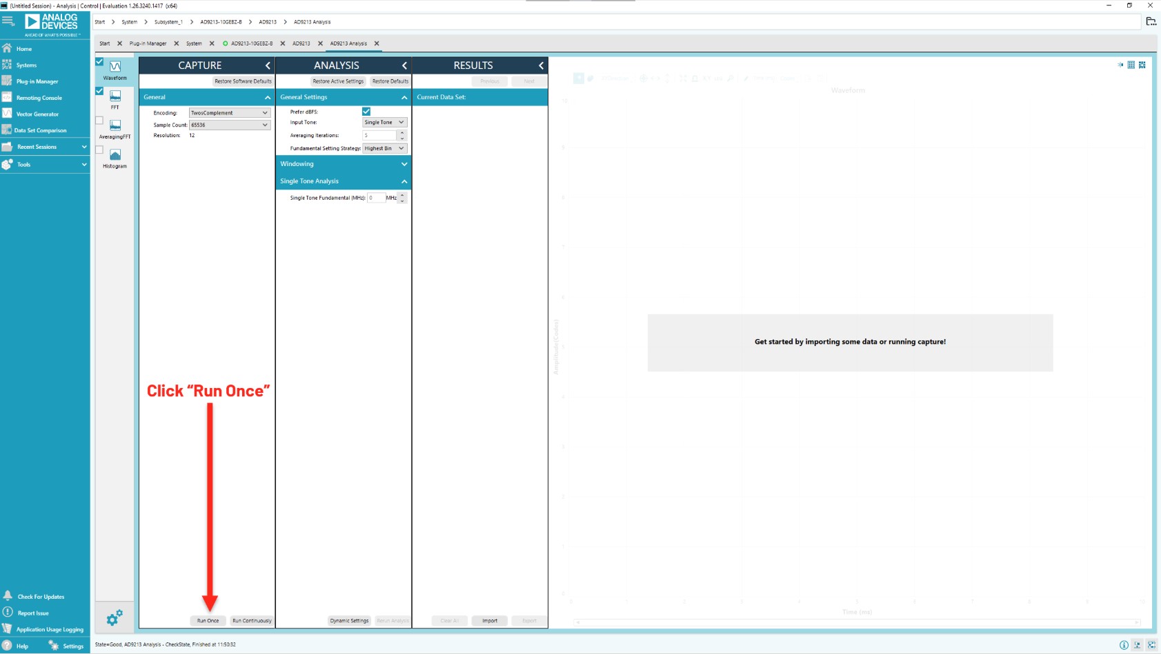
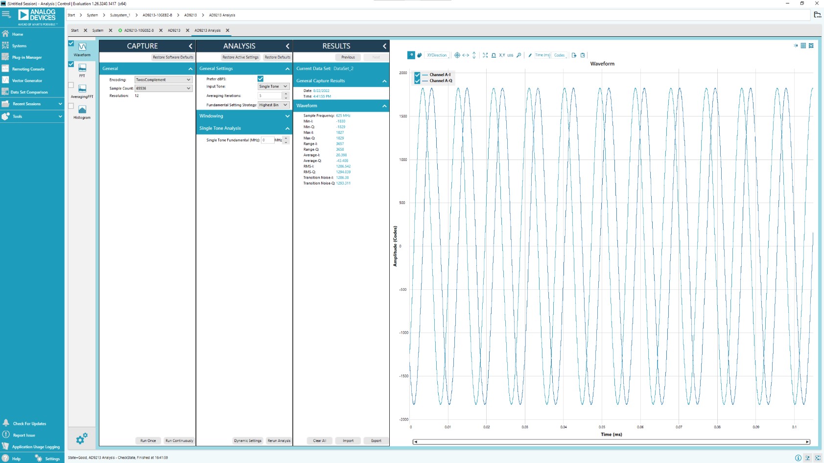
The analysis page appears. Click “Run Once” to get a time domain view at the converted data.
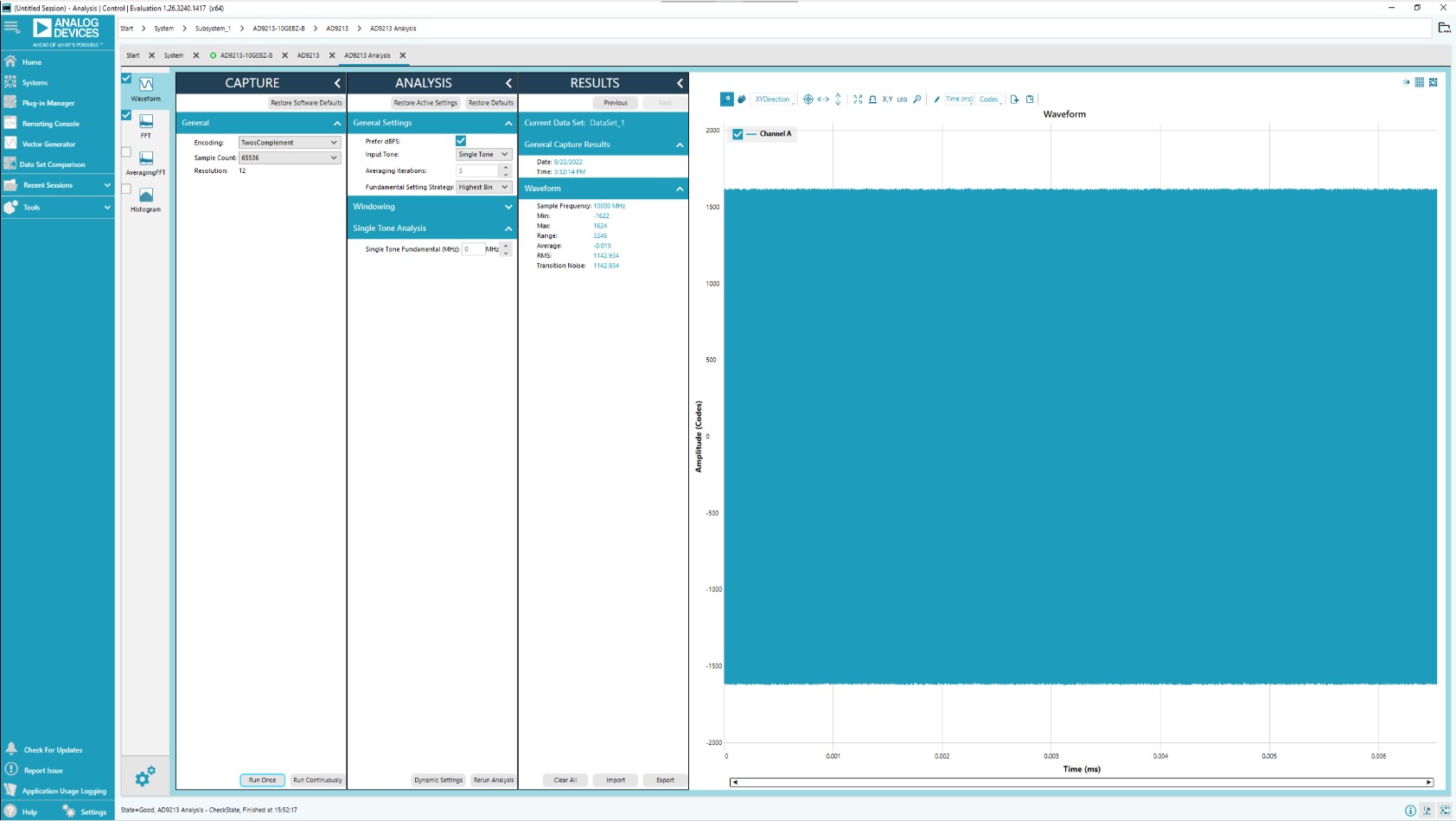
Using the full bandwidth mode setup from step 17, the time domain analysis of converted data appears.
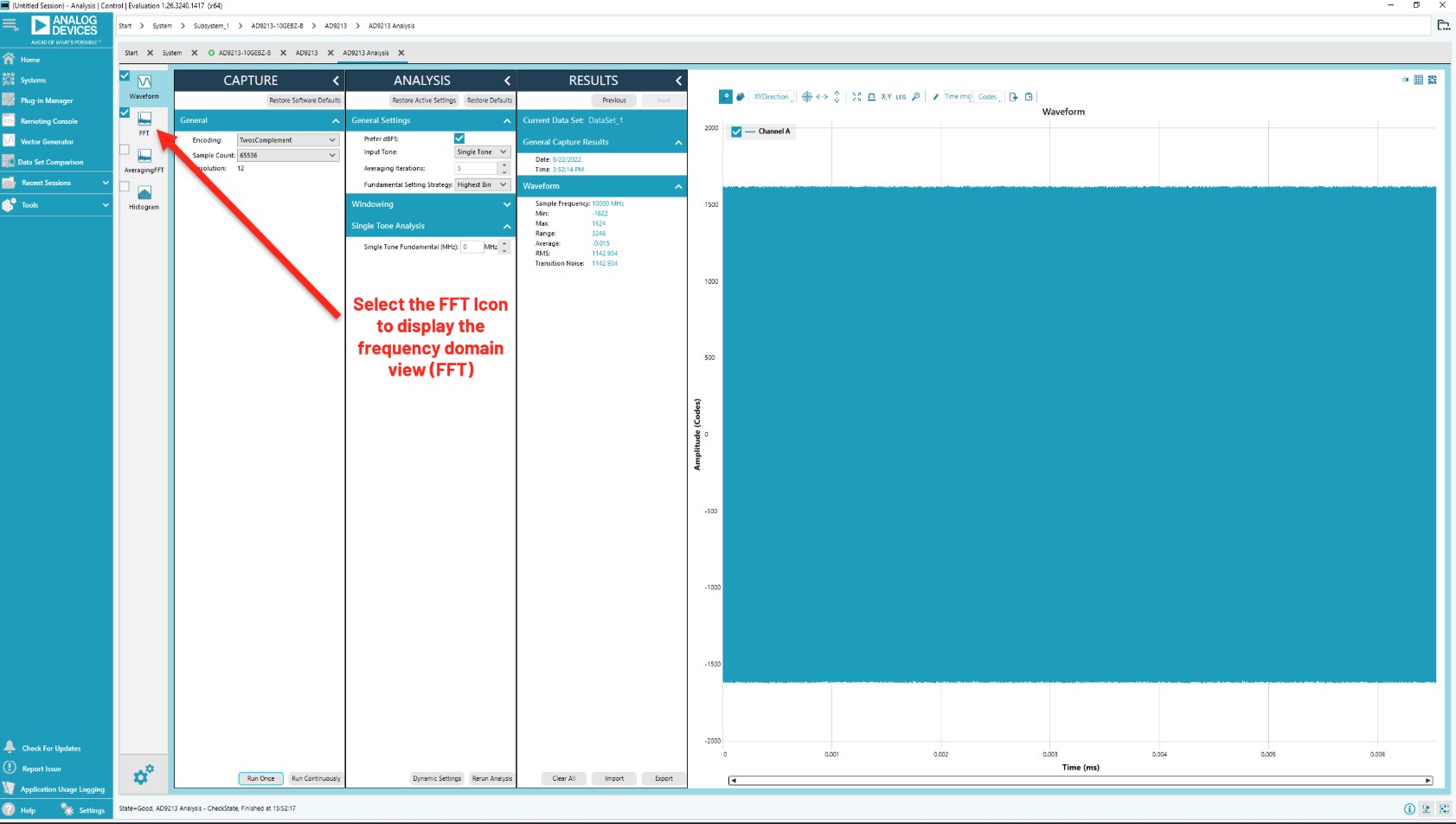
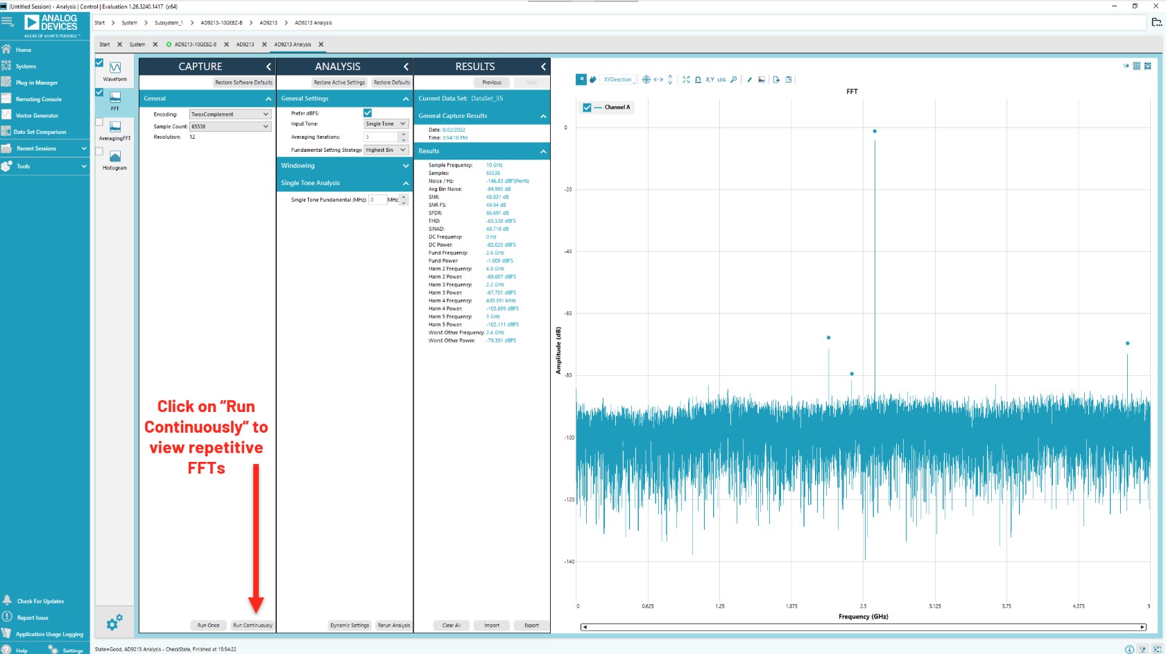
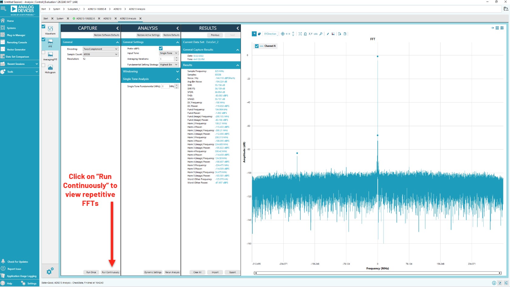
Click on the FFT icon to display the frequency domain view (FFT).
Click “Run Continuously” to view repetitive FFTs.
Using the DDC setup from step 19, the time domain analysis of converted data appears.
Click “Run Continuously” to view repetitive FFTs.
Notes
If the ACE startup procedure does not proceed as described or expected (assuming you properly setup the hardware):
Close the ACE software.
Power down the ADS8-V1EBZ using switch S4.
If after repeated attempts the ACE startup procedure is not successful:
Check that the jumper is placed on the AD9213/9217 evaluation board as shown in step 4.
Check that all signal generators are on and at the correct frequencies and power levels (if external clocks are being used).