AD9209-FMCA-EBZ
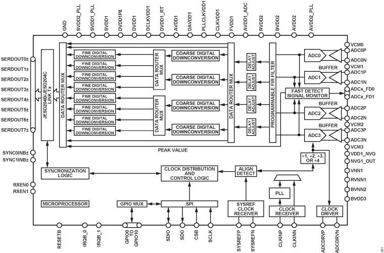
The AD9209 is a quad, 12-bit, 4 GSPS analog-to-digital converter (ADC), similar to ADCs found in the AD9081, AD9082, AD9986, and AD9988 parts. Thus, the evaluation of the AD9209 is done using only the Rx path of the EVAL-AD9081, EVAL-AD9082, EVAL-AD9986, and EVAL-AD9988 evaluation boards.
The AD9209 input features an on-chip wideband buffer with overload protection. This device is designed to support applications capable of direct sampling wideband signals up to 8 GHz. An on-chip, low phase noise, phase-locked loop (PLL) clock synthesizer is available to generate the ADC sampling clock, simplifying the printed circuit board (PCB) distribution of a high frequency clock signal. A clock output buffer is available to transmit the ADC sampling clock to other devices.
Features:
Flexible reconfigurable common platform design
Supports single-, dual-, and quad-band
Datapaths and DSP blocks are fully bypassable
On-chip PLL with multichip synchronization
External RF clock input option for off-chip PLL
Supports clock input frequencies up to 12 GHz
Maximum ADC sample rate up to 4 GSPS
Maximum data rate up to 4 GSPS using JESD204C
8 GHz analog input bandwidth (-3 dB)
ADC ac performance at 4 GSPS
Differential input voltage: 1.4 V p-p
Noise density: -151.5 dBFS/Hz
HD2: -69 dBFS at 2.7 GHz (AIN at -1 dBFS)
HD3: -76 dBFS at 2.7 GHz (AIN at -1 dBFS)
Worst other (excluding HD2 and HD3): -79 dBFS at 2.7 GHz
Auxiliary features
Phase coherent fast frequency hopping
ADC clock driver with selectable divide ratios
On-chip temperature monitoring unit
Flexible GPIOx pins
Versatile digital features
Selectable decimation filters
Configurable DDCs
8 fine complex DDCs and 4 coarse complex DDCs
48-bit NCO per DDC
Programmable 192-tap PFIR filter for receive equalization
Supports 4 different profile settings loaded via GPIO
Programmable delay per datapath
Receive AGC support
Fast detect with low latency for fast AGC control
Signal monitor for slow AGC control
Dedicated AGC support pins
SERDES JESD204B/JESD204C interface, 8 lanes up to 24.75 Gbps
8 lanes per ADC
8 lanes JESD204B/JESD204C Tx (JTx)
Supports real or complex digital data (8-, 12-, 16-, or 24-bit)
15 mm x 15 mm, 324-ball BGA with 0.8 mm pitch
Applications:
Wireless communications infrastructure
Microwave point-to-point, E-band, and 5G mm wave
Broadband communications systems
DOCSIS 3.1 and 4.0 CMTS
Phased array radar and electronic warfare
Electronic test and measurement systems
Recommendations
People who follow the flow that is outlined have a much better experience. However, like many things, documentation is never as complete as it should be. If you have any questions, check the Help and Support section at the bottom of the page.
To better understand the AD9209, we recommend using the EVAL-AD9081, EVAL-AD9082, EVAL-AD9986, or EVAL-AD9988 evaluation boards.
Table of Contents
Block Diagram
Additional Information
Datasheets
Evaluation Software
Project Resources
Help and Support
For additional questions or support, please visit the EngineerZone forum.