CN0535 and the SDP-K1
General Setup
The following sections describe how to set up the CN0535 board using the SDP-K1 and the mbed Example Program for CN0535-FMCZ.
Equipment
SDP-K1 microcontroller board
PC with a USB port and Windows 7 (32-bit) or higher
Serial terminal software (Putty/TeraTerm or similar)
USB standard-A to mini-B cable
6V wall wart power supply
Hardware Setup
The following sections describe the process of setting up the hardware for both the SDP-K1 microcontroller board and the EVAL-CN0535-FMCZ customer evaluation board.
EVAL-CN0535-FMCZ Prep for Use with SDP-K1
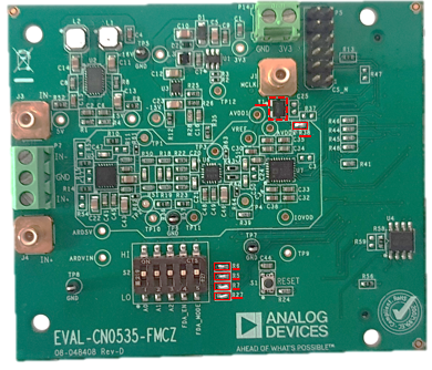
The EVAL-CN0535-FMCZ was designed to be evaluated using SDP-H1. If the user wants to evaluate the CN0535 using SDP-K1, the following components need to be installed. The table below shows the components that the user must install to enable the use of the EVAL-CN0535-FMCZ with the SDP-K1.
Component |
Manufacturing Part Number |
|---|---|
|
TSM-108-04-T-SV |
|
TSM-110-04-T-SV |
|
ERJ-3GEY0R00V or equivalent 0 ohm jumper |
|
0603YC104KAT2A or equivalent |
|
SIT8008BI-21-33E-16.38400G |
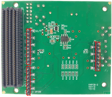
The figures below show the board setup for SDP-K1.
SDP-K1
Shown below is the CN0535 board mounted on the SDP-K1 board via the Arduino headers. The SDP-K1 only requires a single Standard-A to type-C USB cable to connect to the PC. Both the orange Connected LED and green SYS PWR should light on the SDP-K1 if connected correctly.
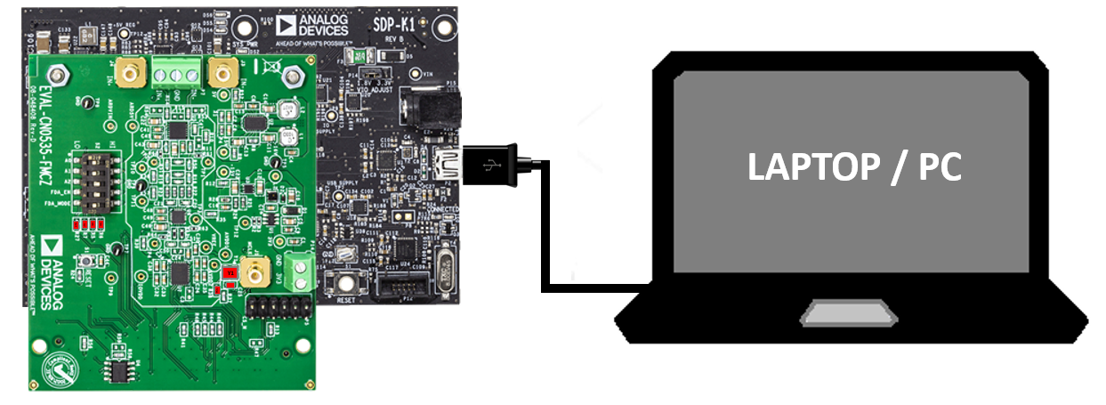
Note
For SDP-K1 Rev E and below, a 6V wall wart power supply is needed on P15.
Software Setup
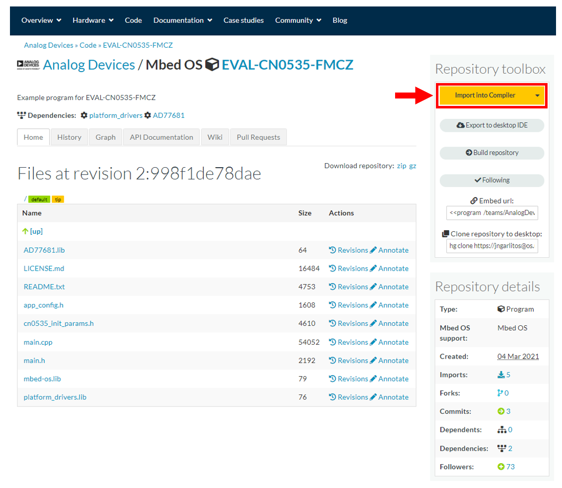
Importing the EVAL-CN0535-FMCZ MBED Example program
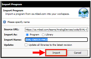
If the user does not have an mbed online account, they must create one at https://ide.mbed.com/.
After having an account, open the Example program for EVAL-CN0535-FMCZ https://os.mbed.com/teams/AnalogDevices/code/EVAL-CN0535-FMCZ/
Connecting to a Serial Terminal Application
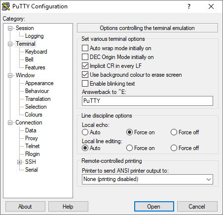
In order to communicate with the board using the SDP-K1, the user needs to install serial terminal software on their PC. It is recommended to use PuTTY, which is available for free download on the internet. The following steps were written with PuTTY in mind; however, any other serial terminal application should follow a similar procedure. The following steps are required to interface with the board.
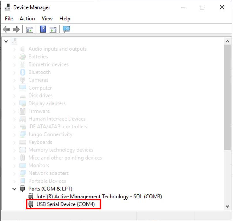
Open Device Manager through the Windows control panel and plug the microcontroller board into the PC. When the board is detected it will appear in Device Manager as USB Serial Device. This also displays the port that the board is connected to. (COM4 in this case)
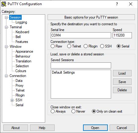
Open the serial terminal application and enter the correct values to configure it to connect to the board. The serial line should be the COM port noted earlier and the speed should be set to 115200 to ensure data transfer works correctly. Also note the changes in the Terminal tab; this is required for the menu to display properly.
Upon connection, the interface menu should appear. If not, press the reset button on the microcontroller board; this will call up the command menu for the user to interact with. (Note: This does not work with version A or B of the SDP-K1.)
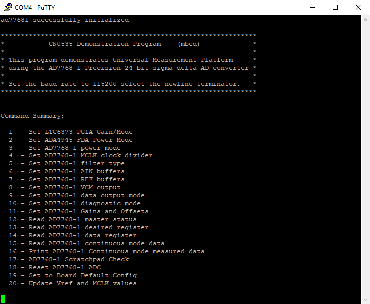
From here, the user should type the number corresponding to their desired choice and press ‘Enter’. Note that many choices will create sub-menus, prompting the user to make another choice.
Command Summary
The following table shows every command along with a brief description. Some commands have recommended settings to apply for optimal results for narrow bandwidth measurements of 32 kHz.
Command |
Description |
|
|---|---|---|
Set LTC6373 PGIA Gain/Mode |
Change the LTC6373 gain or mode. The available options are Shutdown mode and gains of 0.25 V/V, 0.5 V/V, 1 V/V, 2 V/V, 4 V/V, 8 V/V, 16 V/V. |
|
Set ADA4945 FDA Power Mode |
Change the ADA4945 power mode to Full Power Mode or Low Power Mode. |
|
Set AD7768-1 power mode |
Change the AD7768-1 to Low, Medium, or Fast. Low power mode is recommended. |
|
Set AD7768-1 MCLK clock divider |
Change the AD7768-1 clock divider to /16, /8, /4, or /2. /16 is recommended. |
|
Set AD7768-1 filter type |
Change the AD7768-1 filter type used. Also allows the oversampling ratio to be changed. Recommended is the Low ripple FIR filter, oversampled by 32. |
|
Set AD7768-1 AIN buffers |
Adjust the AD7768-1 buffers for both AIN+ and AIN-. It is recommended to turn on both AIN+ and AIN- precharge buffers. |
|
Set AD7768-1 REF buffers |
Adjust the AD7768-1 buffers for both REF+ and REF-. It is recommended to turn on both REF+ and REF- precharge buffers. |
|
Set AD7768-1 VCM output |
Choose the AD7768-1 VCM output voltage. The recommended value is (AVDD1 - AVSS)/2. |
|
Set AD7768-1 data output mode |
Set the AD7768-1 data output mode. |
|
Set AD7768-1 diagnostic mode |
Change which diagnostic mode is used for the ADC. |
|
Set AD7768-1 Gains and Offsets |
Set AD7768-1 gain and offset registers. |
|
Read AD7768-1 main status |
Shows faults in AD7768-1 main status register, allowing the user to pinpoint the source of problems. |
|
Read AD7768-1 desired register |
Reads desired AD7768-1 register. |
|
Read AD7768-1 data register |
Reads AD7768-1 data register. |
|
Read AD7768-1 continuous mode data |
Reads raw data from the ADC over a user-defined number of samples. |
|
Print AD7768-1 Continuous mode measured data |
Prints previously read raw data converted into voltages and codes to the terminal. Logging the terminal output allows the user to extract this data. Requires the ‘Read data’ command to have been run. |
|
AD7768-1 Scratchpad Check |
Input an 8-bit number; if it is returned, the ADC is interfacing with the software. This is a useful quick check for debugging and is good to run after setup. |
|
Reset AD7768-1 ADC |
Resets the ADC, either a soft reset over SPI or hard reset using the reset pin. |
|
Set to Board Default Config |
Set the board to default configurations. |
|
Update Vref and MCLK values |
Update the Vref and MCLK values. |