AD936X Advanced Plugin
The AD936X Advanced plugin (formerly known as the FMCOMMS2/3/4/5 Advanced Plugin) works with the IIO Oscilloscope. You always use the latest version if possible. Changing any field will immediately write changes which have been made to the AD936X settings to the hardware, and then read it back to make sure the setting is valid. If you want to set something that the GUI changes to a different number, that either means that GUI is rounding (sorry), or the hardware (either the AD9361 or the FPGA fabric) does not support that mode/precision.
If you want to go play with /sys/bus/iio/devices/... and manipulate the
devices behind the back of the GUI, it’s still possible to see the settings by
clicking the “refresh” button at the bottom of the GUI.
The AD936X Advanced Plugin allows testing of different device driver initialization options and values. In contrast to the controls on the AD936X Main Plugin– the controls here are not part of the main driver API.
In the No-OS driver the values correspond to members of the setup/init structure. For the AD9361 Linux Device Driver each control corresponds to a specific devicetree property.
See more details about AD9361 Customization.
Tip
After you customized the driver for your application needs you can read back all values from the Linux debugfs:
root@linaro-ubuntu-desktop:~# cd /sys/kernel/debug/iio/iio\:device1/
root@linaro-ubuntu-desktop:/sys/kernel/debug/iio/iio:device1# grep "" * | sed "s/:/ = </g" | awk '{print $0">;"}' adi,2rx-2tx-mode-enable = <1>;
adi,agc-adc-large-overload-exceed-counter = <10>;

[ -- snip -- ]
Simply update the values here: AD9361 Devicetree Initialization
For the No-OS driver the mapping can be found here: AD9361 Customization
Main

Clockout Setting
The Clockout control manages the CLK_OUT pin signal, offering two
configurations:
Buffered external input clock – a digitally controlled crystal oscillator (DCXO) version.
Divided internal ADC sample clock – ADC_CLK with divisor options: /2, /3, /4, /8, /16, /32, /64.
Gain Control

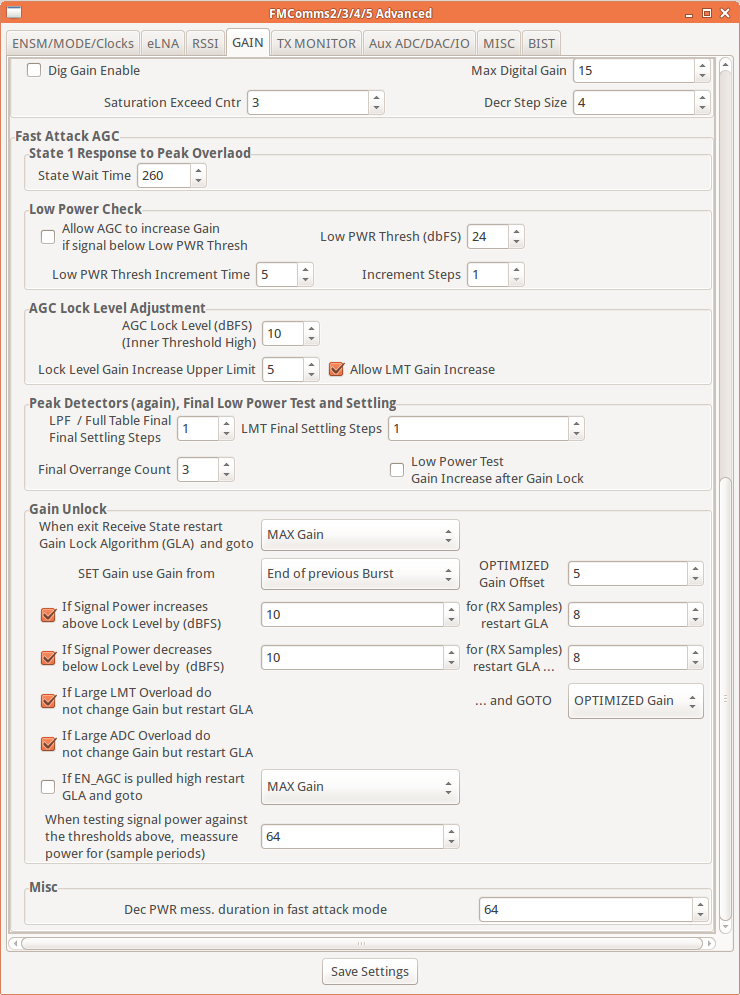
Features three modes with distinct controls:
MGC (Manual Gain Control) – user-adjustable gain.
Slow Attack AGC – automatic gain adjustment with slower response.
Fast Attack AGC – automatic gain adjustment with faster response.
RSSI
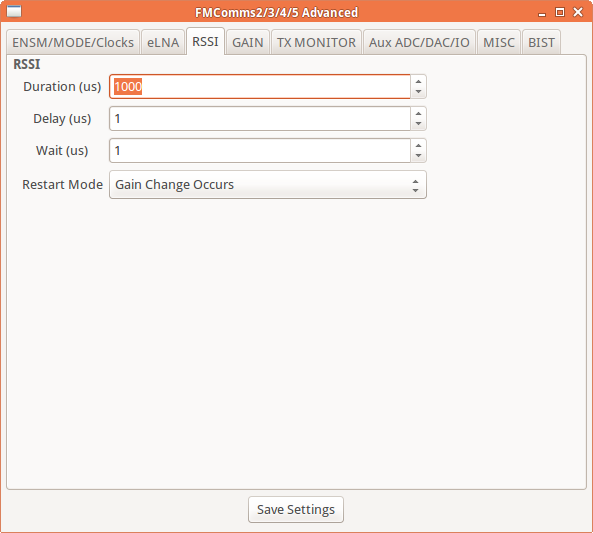
Figure 4 RSSI (Received Signal Strength Indicator) settings.
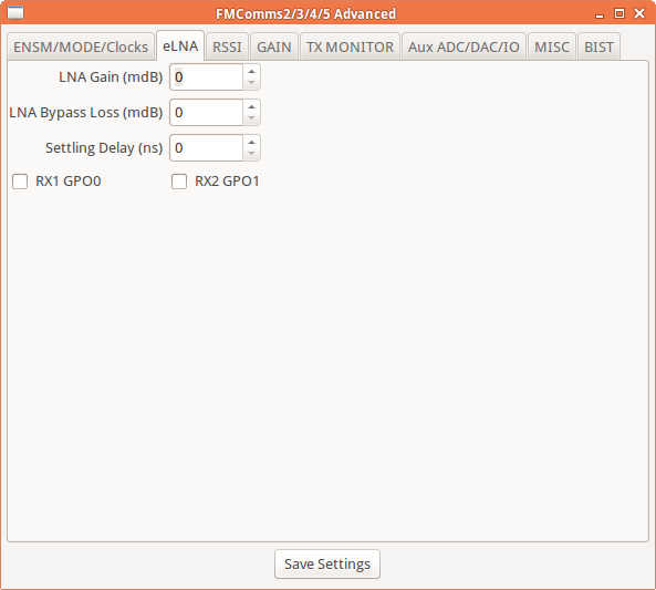
External LNA
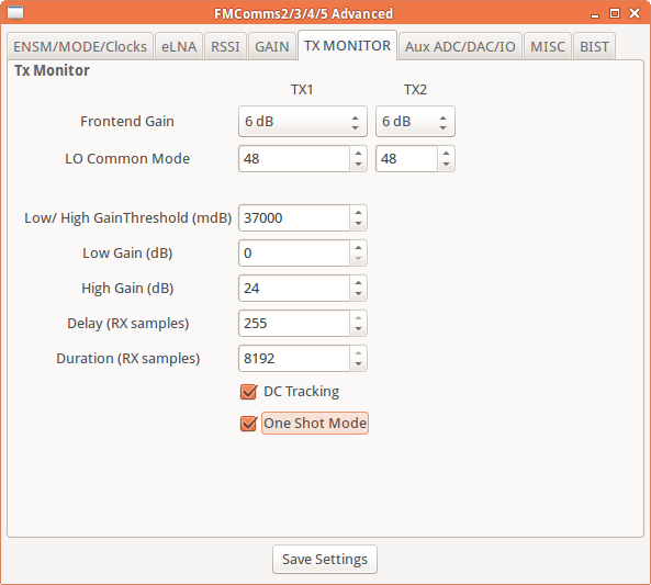
TX Monitor
Auxiliary IO (ADC, DAC, Control IO, Temp Sensor)

Controls for:
ADC (Analog-to-Digital Converter)
DAC (Digital-to-Analog Converter)
Control IO
Temperature Sensor
MISC
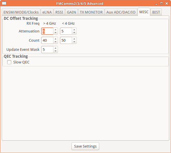
BIST (Built-In Self-Test)
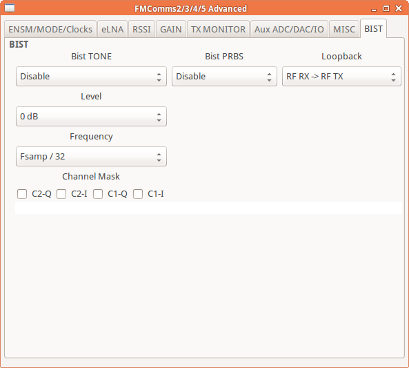
BIST stands for Build-In Self-Test. Selections on this Tab take immediately effect and therefore don’t require the Save Settings Button. Functionality exposed here is only meant to inject test patterns/data than can be used to validate the Digital Interface or functionality of the device.
There are three major facilities. The top most drop down selection box allows you to specify the injection point.
BIST Tone
User-selectable tone with frequency and level selection, injectable into the RX or TX path. Channel masking checkboxes are available: a masked channel (checked box) produces no data output. This is useful for determining the I, Q, Rx1, Rx2 channel-to-data mapping.
BIST PRBS
Pseudorandom Binary Sequence (PRBS) injectable into the RX or TX path.
BIST Loopback
Allows either to digitally loopback TX data into the RX path or vice versa.
Digital TX → Digital RX – the loopback happens inside the AD9361/4 close to the internal digital interface block. The RF section is bypassed. This validates that digital samples/symbols sent to the device are correct.
RF RX → RF TX – the loopback happens in the ADI provided HDL core. The transmitter broadcasts the received signals. The entire RF chain is active, so sample rates, RF bandwidth, and FIR settings all affect the transmission.