DC2903A
LTC2672 Demo Board | Five-Channel Current Output DAC, with Internal Reference and SPI Interface (Requires DC2026C)
Overview
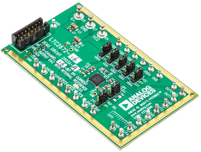
The DC2903A is a fully featured evaluation board that evaluates the LTC2672, a five-channel, current source output digital-to-analog converter (DAC).
The DC2903A is controlled through a serial peripheral interface (SPI) from the J1 connector. The SPI signals are sent from the DC2026C controller board through the ribbon cable that is connected to the DC2903A.
The DC2903A uses QuikEval evaluation software to provide an intuitive graphical user interface (GUI) that configures and controls the LTC2672 using the SPI interface.
The LTC2672 is used for various current mode biasing applications such as tunable lasers or resistive heaters. The output current ranges are softwar selectable, and each channel is routed to the DC2903A MUX pin for external monitoring.
For full specifications on the LTC2672, see the LTC2672 data sheet, which must be consulted in conjunction with the DC2903A user guide when using the DC2903A.
Features
Fully featured evaluation board for the LTC2672
QuikEval evaluation software compatible
Applications
Current mode biasing applications
Evaluating the LTC2672
Supported Evaluation Boards
Hardware Specifications
Power Supply Requirements
The DC2903A board has provision for dual supply operation. The positive voltage supply can range from 2.8V to 5.5V, while the negative supply voltage can handle voltages from -5.5V up to 0V or GND. To ensure proper operation, make sure that the supply used can source at least the total maximum current expected from each channel.
If the maximum current output expected from each channel is 300 mA, then the supply used should be able to source at least 1500 mA (for example, 300 mA x 5 channels) to operate the device properly across all available span and current levels.
Digital Interface (QuikEval)
The QuikEval system is a USB-based product demonstration and data acquisition system that allows users to quickly evaluate the performance of Linear Technology products, including the LTC2672. Its interface is a 14-pin connection that allows the Linduino to connect with over a hundred Analog Devices daughter boards for parts including analog-to-digital converters, digital-to-analog converters, high-voltage power monitors, temperature measurement devices, RF synthesizers, battery stack monitors, and more.
The specific interface used for the DC2903A boards is SPI.
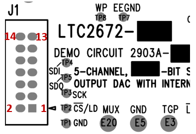
P1 Pin Number |
Pin Function |
Mnemonic |
|---|---|---|
Pin 1 |
+7V. Unregulated |
7V |
Pin 2 |
I/O Voltage |
IOVDD |
Pin 3 |
Board Ground |
GND |
Pin 4 |
Serial Clock |
SCLK |
Pin 5 |
Main In Subordinate Out |
MISO |
Pin 6 |
Chip Select |
CS |
Pin 7 |
Main Out Subordinate In |
MOSI |
Pin 8 |
Board Ground |
GND |
Pin 9 |
EEPROM SDA (I2C) |
EESDA |
Pin 10 |
EEPROM VCC |
EEVCC |
Pin 11 |
EEPROM SCL (I2C) |
EESCL |
Pin 12 |
EEPROM Ground |
GND |
Pin 13 |
Board Ground |
GND |
Pin 14 |
Free GPIO |
GPIO |
The follow pins have alternate function:
Serial Clock is for either SPI or I2C.
Main Out Subordinate In or MOSI also acts as SDA pin for I2C mode.
ADI No-OS
The goal of ADI Microcontroller No-OS is to provide reference projects for lower end processors, which can’t run Linux or aren’t running a specific operating system, and to help those customers using microcontrollers with ADI parts. ADI No-OS offers generic drivers, which can be used as a base for any microcontroller platform and also example projects, which are using these drivers on various microcontroller platforms.
For more information about ADI No-OS and supported microcontroller platforms, visit the No-OS User Guide found no-os.
LTC2672 Driver
Information about the LTC2672 driver can be found here: LTC2672 No-OS Driver
No-OS Supported Platforms
Maxim Platform
Hardware Setup
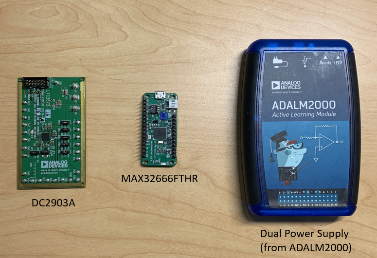
Required Hardware
Dual Power Supply
Required Connections
The MAX32666FTHR does not have a PMOD interface, but you may use Dupont female-female cables to make the required connections. The table below shows the connection between DC2903A and MAX32666FTHR.
DC2903A Pin Number |
MAX32666 Pin Number |
Function |
Mnemonic |
|---|---|---|---|
Pin 1 |
3V3. |
3.3V Supply (for IO) |
3V3 |
Pin 3 |
GND. |
Board Ground |
GND |
SCK |
AIN3 |
Serial Clock |
SCLK |
SDI |
AIN1 |
Main In Subordinate Out |
MISO |
CS/LO |
AIN0 |
Chip Select |
CS |
SDO |
AIN2 |
Main Out Subordinate In |
MOSI |
After connecting the pins from the DC2903A QuikEval interface to the MAX32666FTHR’s pins, connect the corresponding pins to VCC, V-, and GND. Make sure that the voltages to these pins are within the normal operating range. Power up the supplies in any order as the device doesn’t need any sequencing.
No-OS Build Setup
To build the example project, follow the instructions in the no-OS User Guide found here.
Example Project Execution
Basic Example Project
The basic project contains the generic HAL initialization of the used platform, together with the SPI, and UART driver configuration and initialization.
The SPI driver is used to communicate with the DC2903A device and change its settings, and the UART driver is used to display on the host machine the device configuration at a given instance.
The basic project contains the LTC2672 driver initialization and project functions:
/* Continuously configure the part and measure pins with multimeter for
verification */
    while (1) {
        /*max current of 3.125mA*/
        ret = ltc2672_set_span_all_channels(ltc2672_desc,
                            LTC2672_50VREF);
        if (ret) {
            goto error;
        }

        /* Print Span set to all channels */
        pr_info("All DAC channels have span config of 3.125mA\n");

        for (i = 0; i < num_currents; i++) {
            ret = ltc2672_set_current_all_channels(ltc2672_desc,
            currents_to_set[i]);
            if (ret) {
                goto error;
            }

            /* Print Current set to all channels */
            pr_info("All DAC channels have current of: %0.2f mA\n",
            currents_to_set[i]);

            /*Lengthy delay to better visualize the change in values*/
            no_os_mdelay(1500);
        }

        /* Configure MUX pin to output the VREF measurement */
        pr_info("MUX ouptut pin configured to measure VREF (~1.25V).\n");

        ret = ltc2672_monitor_mux(ltc2672_desc, LTC2672_MUX_VREF);
        if (ret) {
            goto error;
        }

        /*Lengthy delay to better visualize the change in values*/
        no_os_mdelay(2000);

        /* Chip Power Down */
        pr_info("Chip Power Down. All Channels and VREF should measure 0.\n");

        ret = ltc2672_chip_power_down(ltc2672_desc);
        if (ret) {
            goto error;
        }

        /*Lengthy delay to better visualize the change in values*/
        no_os_mdelay(2000);

        /* Setup and Demo toggle function on OUT3 */
        pr_info("Toggle function on OUT3. Current toggles between %0.2f and %0.2f mA.\n",
            currents_to_toggle[0], currents_to_toggle[1]);

        ret = ltc2672_setup_toggle_channel(ltc2672_desc, LTC2672_DAC3,
                           currents_to_toggle[0], currents_to_toggle[1]);
        if (ret) {
            goto error;
        }

        ret = ltc2672_enable_toggle_channel(ltc2672_desc, 8);
        if (ret) {
            goto error;
        }

        for (i = 0; i < toggle_times; i++) {
            toggle_flag ^= true;

            ret = ltc2672_global_toggle(ltc2672_desc, toggle_flag);
            if (ret) {
                goto error;
            }

            /*Lengthy delay to better visualize the change in values*/
            no_os_mdelay(2000);
        }

        ret = ltc2672_enable_toggle_channel(ltc2672_desc, 0);
        if (ret) {
            goto error;
        }

        /*Lengthy delay to better visualize the change in values*/
        no_os_mdelay(2000);

    }// end while
Project Execution
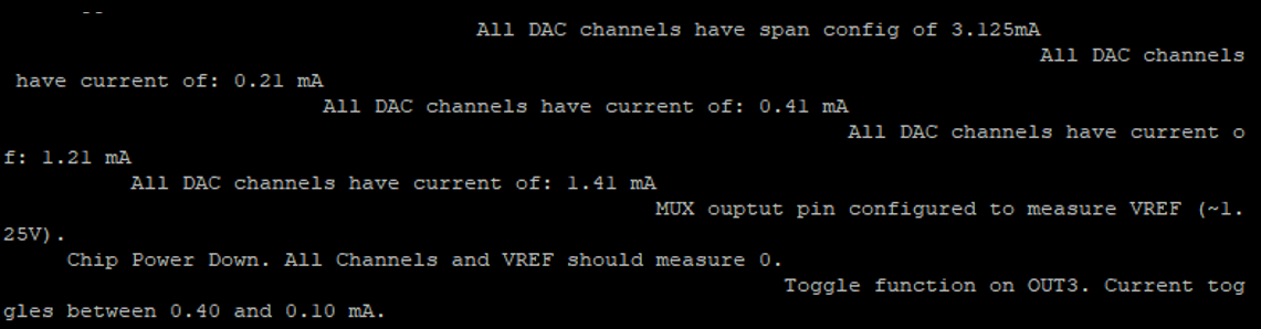
Serial output when running the basic project:
All DAC channels have span config of 3.125 mA
All DAC channels have current of: 0.21 mA
All DAC channels have current of: 0.41 mA
All DAC channels have current of: 1.21 mA
All DAC channels have current of: 1.41 mA
MUX ouptut pin configured to measure VREF (~1.25V).
Chip Power Down. All Channels and VREF should measure 0.
Toggle function on OUT3. Current toggles between 0.40 and 0.10 mA.
Hardware Output Checking
Here are the steps on checking the hardware output when using the example code.
Connect the DC2903A to the MAX32666FTHR microcontroller board by following the required connections in Hardware Setup section.
Build and load the example HEX file to the microcontroller board.
Reset or reconnect the microcontroller board to the computer or a power supply.
Using a DC ammeter, check all channels (OUT0~OUT3) for current readings.
Using a DC voltmeter, measure the voltage on MUX pin; it should read ~1.25V.
Using a DC ammeter, measure the changes in current on OUT3; it should sequentially read ~0.21A, ~0.41A, ~1.21A, ~1.41A.
A power down command should come after the above sequence. During this state, OUT3 should read ~0A.
A toggle command will execute after powering down. During this state, OUT3 should sequentially read ~0.4A, ~0.1A.
Repeat the processes above to confirm functionality.
Note
The example project runs sequentially and continuously repeats the process until power is removed.
More Information and Useful Links
Warning
All the products described on this page include ESD (electrostatic discharge) sensitive devices. Electrostatic charges as high as 4000V readily accumulate on the human body or test equipment and can discharge without detection. Although the boards feature ESD protection circuitry, permanent damage may occur on devices subjected to high-energy electrostatic discharges. Therefore, proper ESD precautions are recommended to avoid performance degradation or loss of functionality. This includes removing static charge on external equipment, cables, or antennas before connecting to the device.
Help and Support
Please go to Help and Support page.