User guide
This user guide describes the AD9656 evaluation board EVAL-AD9656, which provides the support circuitry required to operate the ADC in its various modes and configurations.
The AD9656 data sheet provides additional information and should be consulted when using the evaluation board.
Evaluation board hardware
The evaluation board provides the support circuitry required to operate the AD9656 in its various modes and configurations. It is critical that the signal sources used for the analog input and clock have very low phase noise (ideally ~100 fs rms jitter) to realize the optimum performance of the signal chain. Proper filtering of the analog input signal to remove harmonics and lower the integrated or broadband noise at the input is necessary to achieve the specified noise performance.
Hardware configuration
Set the jumper settings/link options on the evaluation board for the required operating modes before powering on the board. The functions of the jumpers are described in the table below. The default jumper settings are shown in Figure 1.
Jumper |
Description |
|---|---|
P101, P103 |
These jumpers determine the power source for the AD9656EBZ.
|
J304 |
This jumper enables the on-board crystal oscillator. Remove this jumper (and optionally C302) if an external off-board clock source is used. |
J206 |
This jumper selects between internal VREF and external VREF.
|
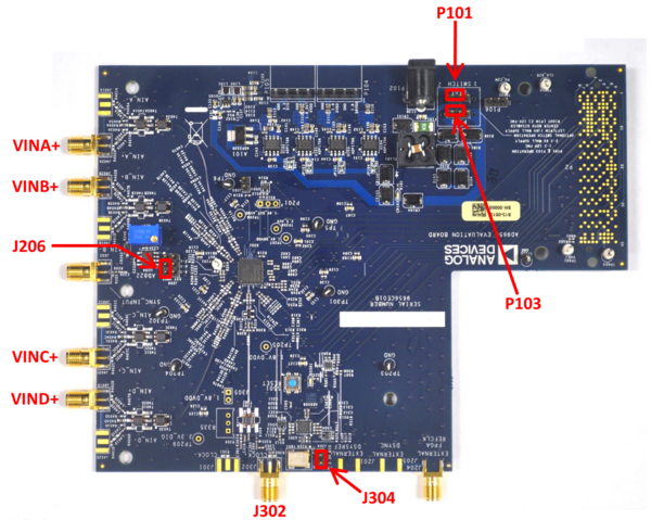
Figure 1 Default Jumper Connections for EVAL-AD9656 Board
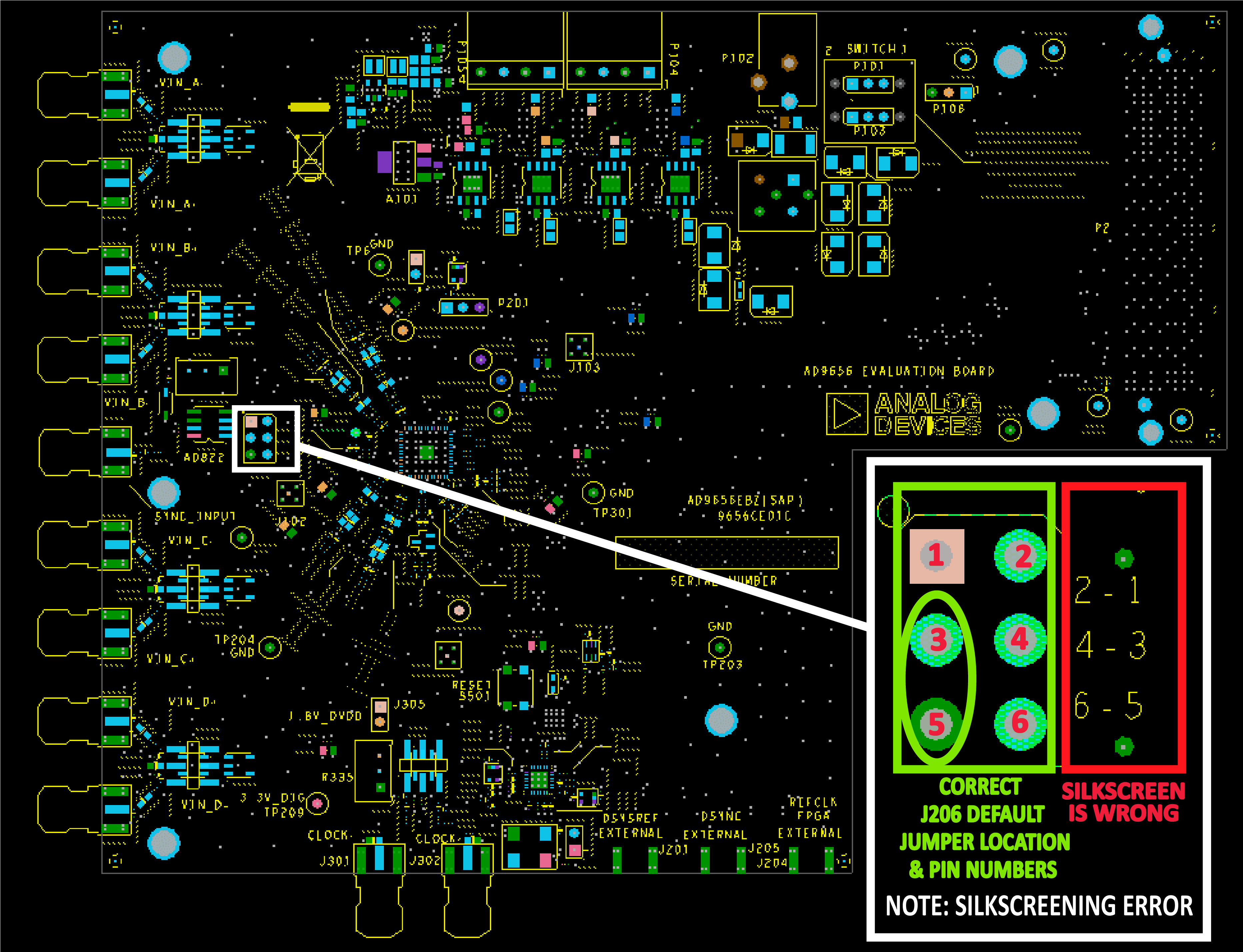
Figure 2 Silkscreen error on 9656CE01C board — the correct numbering is shown in the green box.
Power supply
The EVAL-AD9656 can be powered in one of three ways:
FMC connector power (default)
The default configuration powers the board through the FMC connector from the carrier board. P101 and P103 both need to have Pin 1 tied to Pin 2. If P101 and P103 have Pin 1 jumpered to Pin 2, do not connect the supplied 6V wall supply to the AD9656 evaluation board. When changing the configuration of P101 and P103, please remove both jumpers and then place them in their desired positions.
Wall supply power
Alternatively, the board can obtain its power from the wall-mountable 6V, 2A switching power supply. For this mode, P101 and P103 both need to have Pin 2 tied to Pin 3. Connect the supply to a 100V ac to 240V ac, 47Hz to 63Hz wall outlet. The output from the supply is provided through a 2.1mm inner diameter jack that connects to the PCB at P102. The 6V supply is fused and conditioned on the PCB before connecting to the low dropout linear regulators that supply the proper bias to each of the various sections on the board.
External bench power supplies
The evaluation board can also be powered using external bench power supplies. To do this, remove the E104, E105, E106, and E108 ferrite beads to disconnect the on-board LDOs from the power planes. Note that in some board configurations some of these might already be uninstalled. P104 and P105 headers can be installed to facilitate connection of external bench supplies to the board. E110, E111, E112 and E113 need to be populated to connect P104 and P105 to the board power domains. A 1.8V, 0.5A supply is needed for 1.8V_DUT_AVDD, 1.8V_DRVDD and 1.8V_DVDD. Although the voltage requirements are the same for these three, it is recommended that separate supplies be used for each of these. A 3.3V, 0.5A supply is needed for 3.3V_DIG, which is used to power additional on-board circuitry.
Analog inputs
The four channel inputs on the evaluation board are set up for a double balun-coupled analog input with a 50Ω impedance. When connecting the ADC clock and analog source, use clean signal generators with low phase noise, such as the Rohde & Schwarz SMA, or an equivalent. Use a shielded, RG-58, 50Ω coaxial cable (optimally 1 m or shorter) for connecting to the evaluation board. Enter the desired frequency and amplitude (see the Specifications section in the data sheet). When connecting the analog input source, use of a multipole, narrow-band band-pass filter with 50Ω terminations is recommended. Analog Devices uses band-pass filters from TTE and K&L Microwave, Inc. Connect the filters as close to the evaluation board as possible.
Clock
The default clock input circuit is derived from an on-board 125MHz crystal oscillator feeding through a transformer-coupled circuit using a high bandwidth 1:1 impedance ratio transformer (T302) that adds negligible jitter to the clock path. The external clock input (J302) is 50Ω terminated and ac-coupled to handle single-ended sinusoidal inputs. The transformer converts the single-ended input to a differential signal that is clipped by CR301 before entering the ADC clock inputs. The AD9656 ADC is equipped with an internal clock divider (programmable divide ratios of 1 through 8) to facilitate usage with higher frequency clocks. When using the internal divider and a higher input clock frequency, remove CR301 to preserve the slew rate of the clock signal.
The EVAL-AD9656 board is set up to be clocked through the transformer-coupled input network from the 125MHz crystal oscillator, Y801. If an external clock source is desired, remove C302 (optionally) and Jumper J304 to disable the oscillator from running and connect the external clock source to the SMA connector, J302 (labeled CLOCK+).
If an external clock source is used instead of the onboard crystal oscillator, it should also be supplied with a clean signal generator as previously specified for the analog input signals. Analog Devices evaluation boards typically can accept ~2.8V p-p or 13 dBm sine wave input for the clock at the board SMA clock connector.
Output signals
The JESD204B outputs from the ADC are routed to P2 using 100Ω differential traces.
Schematic, PCB Layout, Bill of Materials
These diagrams demonstrate the routing and grounding techniques that should be applied at the system level when designing application boards using these converters.
Software guide
The EVAL-AD9656 platform development environment supports no-OS applications and IIO interfaces.
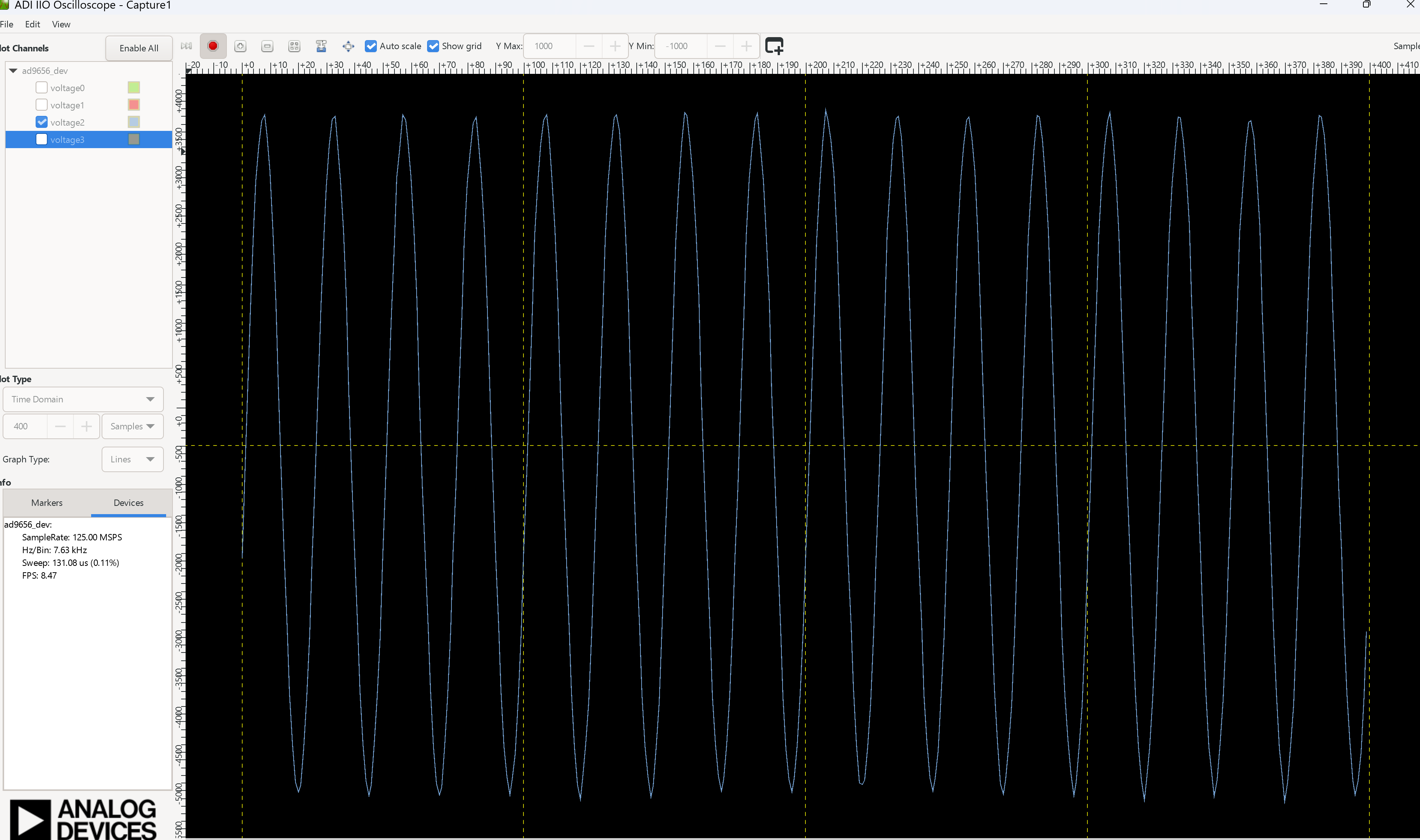
ADI IIO Oscilloscope
The IIO Oscilloscope is a cross-platform application for interfacing with IIO devices, enabling you to configure device parameters and visualize data.
Important
Make sure to download/update to the latest version of IIO Oscilloscope.
For no-OS
For connecting IIO Oscilloscope to no-OS applications, they need to be built with the IIOD=y flag. This way, the no-OS applications will run an IIO daemon that is awaiting connections from the IIO Oscilloscope.
As indicated in the boot log, the board runs an IIOD server over the serial (UART) connection.
Disconnect or close the serial terminal used to view the boot log.
Once done with the installation or an update of the latest IIO Oscilloscope, open the application.
Select the Serial backend and configure the connection with the settings shown at the end of the boot log.
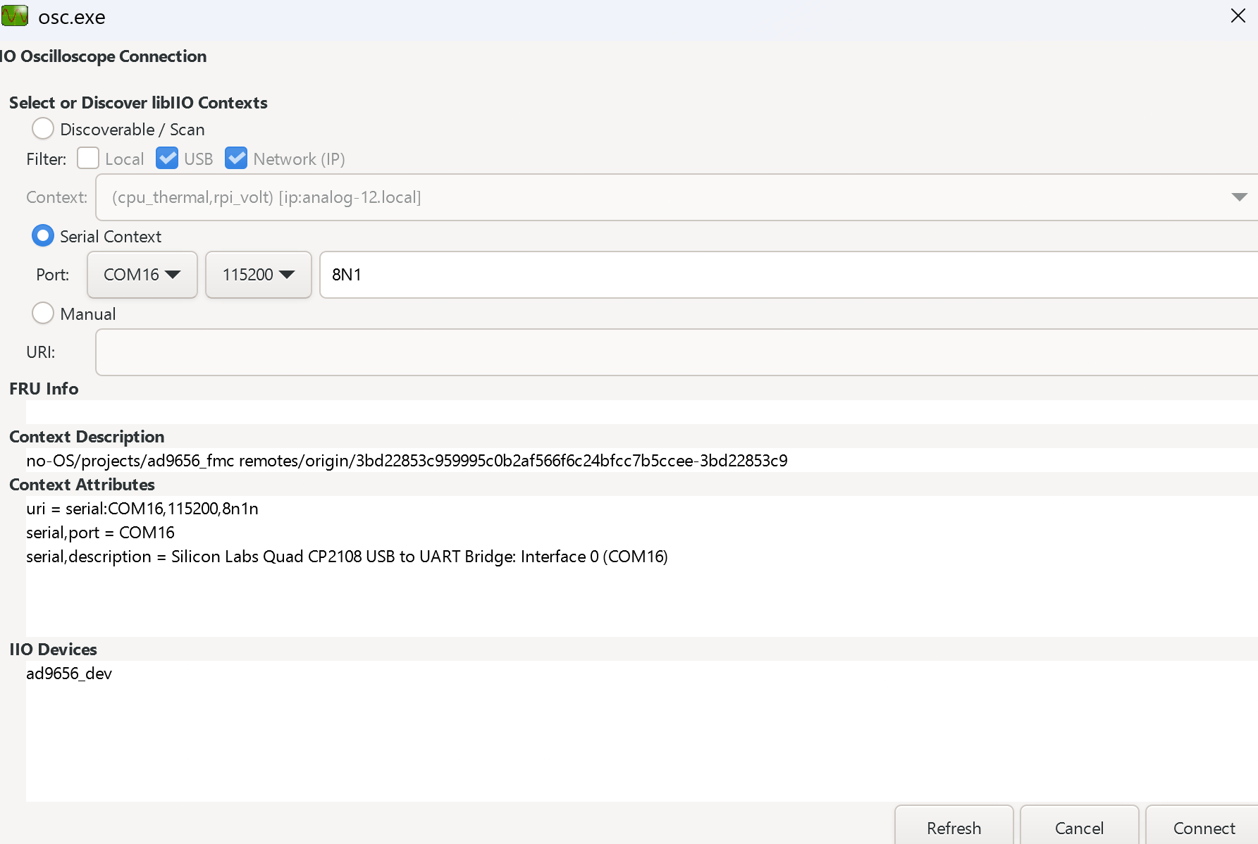
Press Refresh to display the available IIO devices and press Connect.
Note
The serial port is the COM port on Windows or /dev/ttyUSBx on Linux.
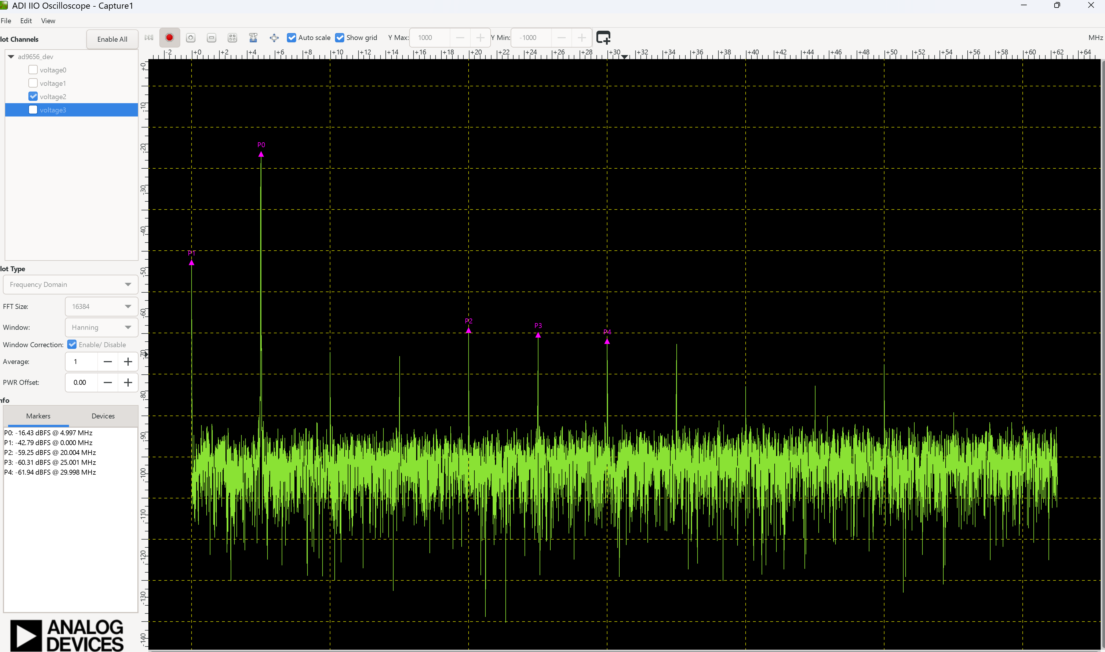
Data capture
Note
Device names and channel definition may differ between no-OS and Linux.
Time domain:
Frequency domain: