AD-FMCOMMS1-EBZ Specifications
Warning
Analog Devices uses six designations to inform our customers where a semiconductor product is in its life cycle. From emerging innovations to products which have been in production for twenty years, we understand that insight into life cycle status is important. Device life cycles are tracked on their individual product pages on analog.com, and should always be consulted before making any design decisions.
This particular article/document/design has been retired or deprecated, which means it is no longer maintained or actively updated, even though the devices themselves may be Recommended for New Designs or in Production. This page is here for historical/reference purposes only.
Transmit Specs
There are many specifications on the Transmit side of a RF system
Theoretical specs
Bandwidth
Determining overall channel bandwidth is a little complex, since many devices don’t have a meaningful (in this aspect) bandwidth number.
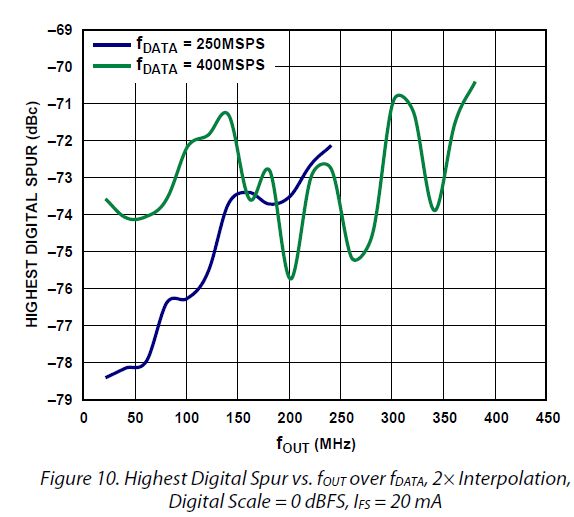
In the AD9122, the above figure shows an fDATA of 400MHz, creating a waveform over 350MHz.
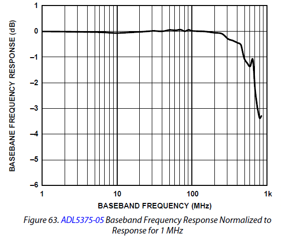
The ADL5375 does include a baseband bandwidth specification - depending on the flatness you require, could be 200MHz (+/- 0.1dB) or 500MHz (+/- 0.5dB).
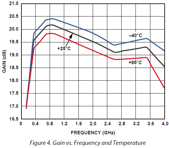
the ADL5602 has different gain, depending on the RF frequency (but over 250MHz, you will still notice).
So, transmit bandwidth can be as high as 250 MHz, depending on if the flatness of the ADL5602 and ADL5375 works for your application.
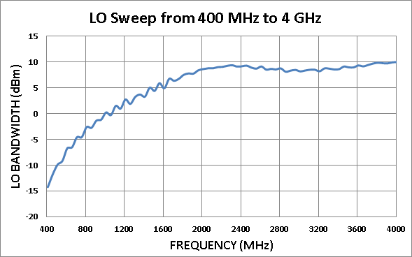
LO BW (Modified Board)
|
Adjacent Channel Power (Modified Board)
|
|
ACP with LO of 1.2GHZ and Tone of 40MHz with full power out. |
ACP with LO of 1.2GHZ and Tone of 40MHz with half power out. |


|
|
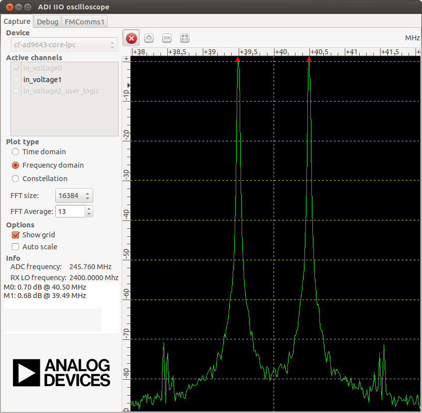
ACP with LO of 2.4GHZ and Tone of 40MHz with full power out. |
ACP with LO of 2.4GHZ and Tone of 40MHz with half power out. |


|
|
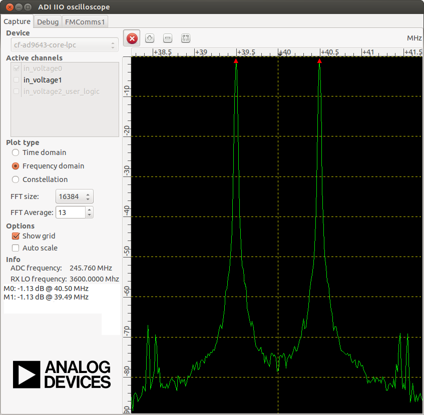
ACP with LO of 3.6GHZ and Tone of 40MHz with full power out. |
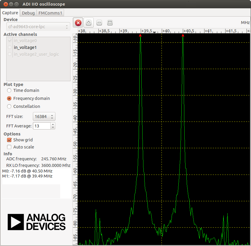
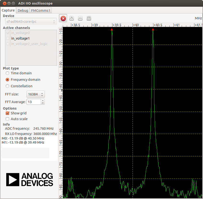
ACP with LO of 3.6GHZ and Tone of 40MHz with half power out. |


Phase Noise (RevB unmodified Board)
|
|
Phase Noise at LO of 400MHz and Tone of 40MHz with full power out. |
Phase Noise at LO of 900MHz and Tone of 40MHz with full power out. |


|
|
Phase Noise at LO of 1.8GHz and Tone of 40MHz with full power out. |
Phase Noise at LO of 2.4GHz and Tone of 40MHz with full power out. |


|

Phase Noise (RevB Modified Board & RevC)
|
|
Phase Noise at LO of 1.2GHz and Tone of 40MHz with full power out. |
Phase Noise at LO of 1.2GHz and Tone of 40MHz with half power out. |


|
|
Phase Noise at LO of 2.4GHz and Tone of 40MHz with full power out. |
Phase Noise at LO of 2.4GHz and Tone of 40MHz with half power out. |


|
|
Phase Noise at LO of 3.6GHz and Tone of 40MHz with full power out. |
Phase Noise at LO of 3.6GHz and Tone of 40MHz with half power out. |


Output power (Modified Board)
|

|

|

Intermodulation Distortion (Old Board)
Intermodulation_Distortion or IMD
|
|
Intermodulation Distortion showing 3rd and 5th order products at 450MHz for 3 power levels |
Intermodulation Distortion showing 3rd and 5th order products at 950MHz for 3 power levels |
|
|
Intermodulation Distortion showing 3rd and 5th order products at 1.85GHz for 3 power levels |
Intermodulation Distortion showing 3rd and 5th order products at 2.45GHz for 3 power levels |
Intermodulation Distortion (Modified Board)
|
|
|
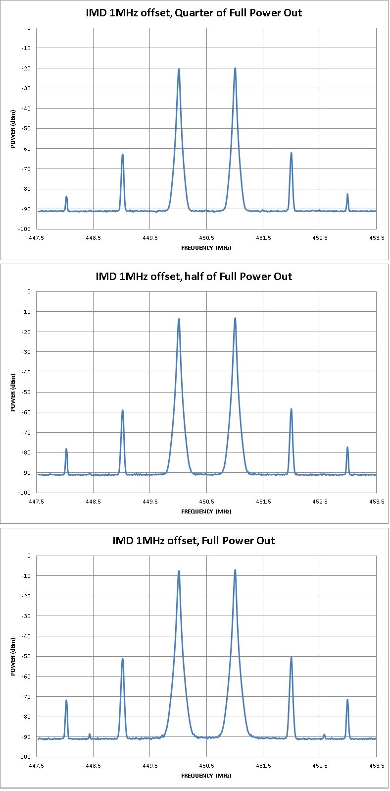
1MHz Offset, LO 1.2GHz, Scale of 0.5 |
1MHz Offset, LO 1.2GHz, Scale of 0.25 |
1MHz Offset, LO 1.2GHz, Scale of 0.125 |
|
|
|
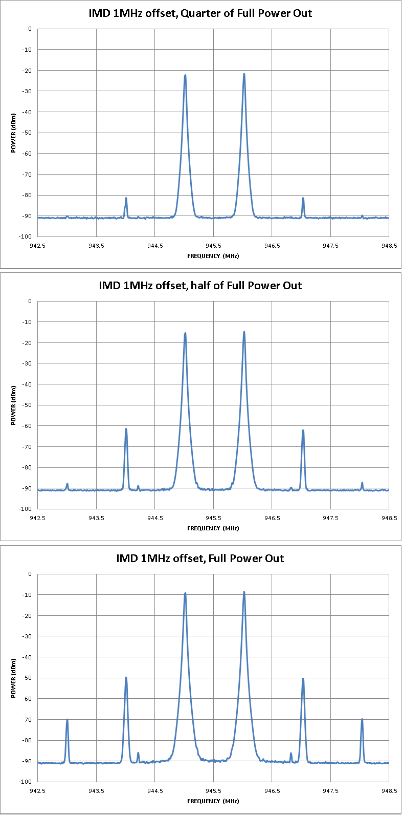
1MHz Offset, LO 2.4GHz, Scale of 0.5 |
1MHz Offset, LO 2.4GHz, Scale of 0.25 |
1MHz Offset, LO 2.4GHz, Scale of 0.125 |
|
|
|
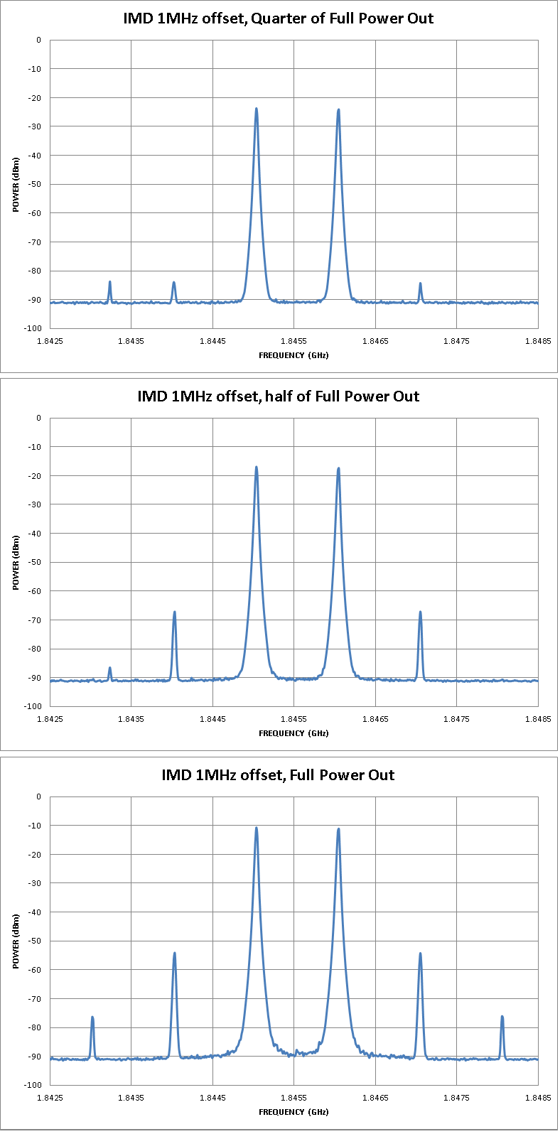
1MHz Offset, LO 3.6GHz, Scale of 0.5 |
1MHz Offset, LO 3.6GHz, Scale of 0.25 |
1MHz Offset, LO 3.6GHz, Scale of 0.125 |


bandwidth (Modified Board)
|

|

|

Receive Specs
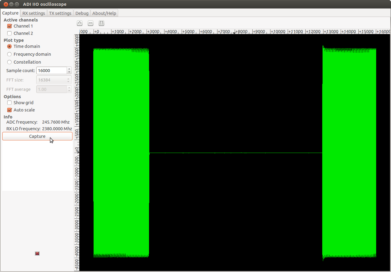
Response to a “chirp”
Although this doesn’t have a specific number associated with it, many RF systems are “chirpy” - and linear response to these RF pulses is very important.
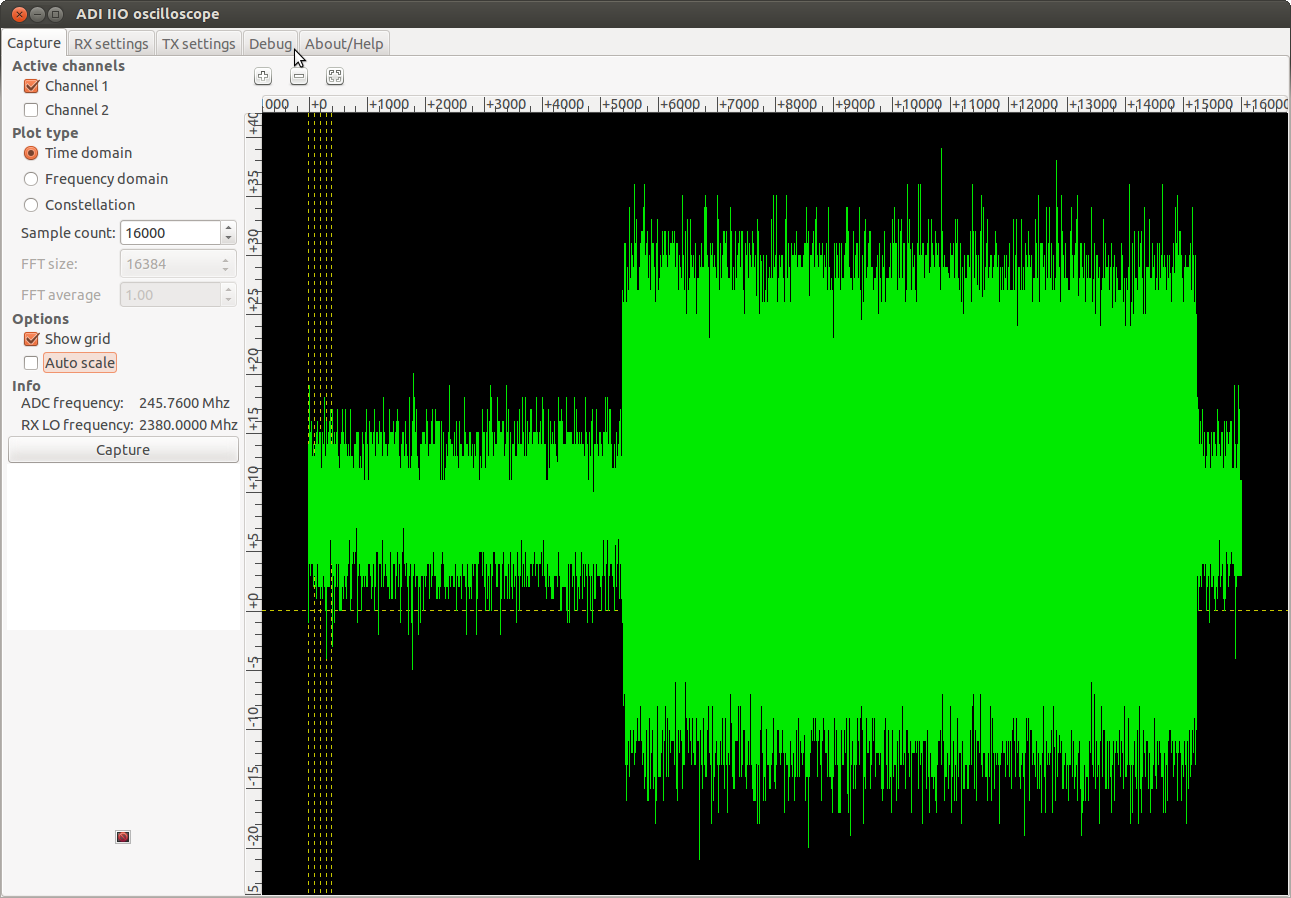
Here is a 2.4GHz waveform, input at -60dbB, with the VGA gain turned up to +20dB. Although this does have some DC offset (the card was not calibrated), the response is very linear over time, even when zoomed in. (Clicking on either picture will open it up in a larger window)
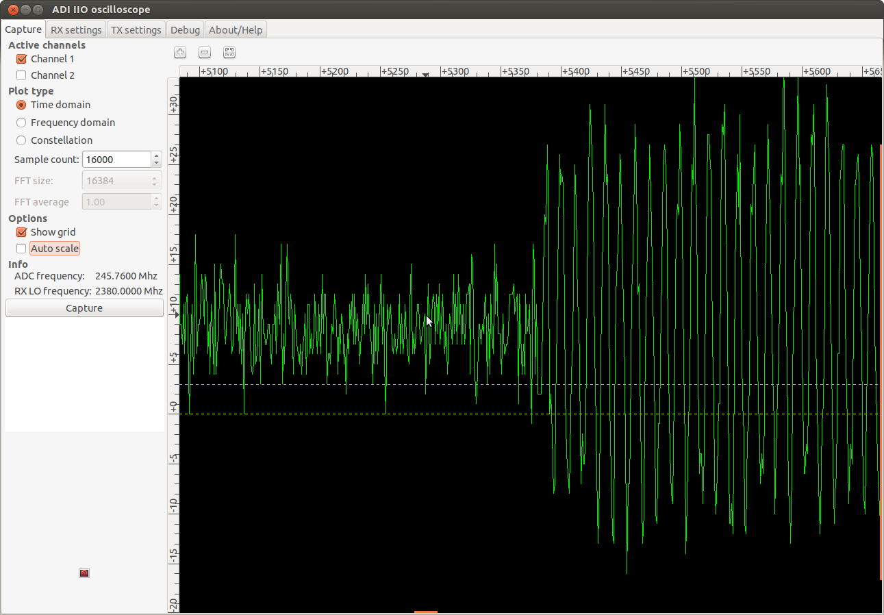
And with a larger input - it looks similar. This is with an input of +6.0dBm, with the VGA set to 4.5dB.|
The results are similar at different frequencies.|
Signal to Noise
Noise floor
Input sensitivity
Dynamic range
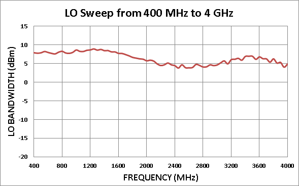
LO BW (Modified Board)
|
|
Intermodulation Distortion (Modified Board)
|
|
|
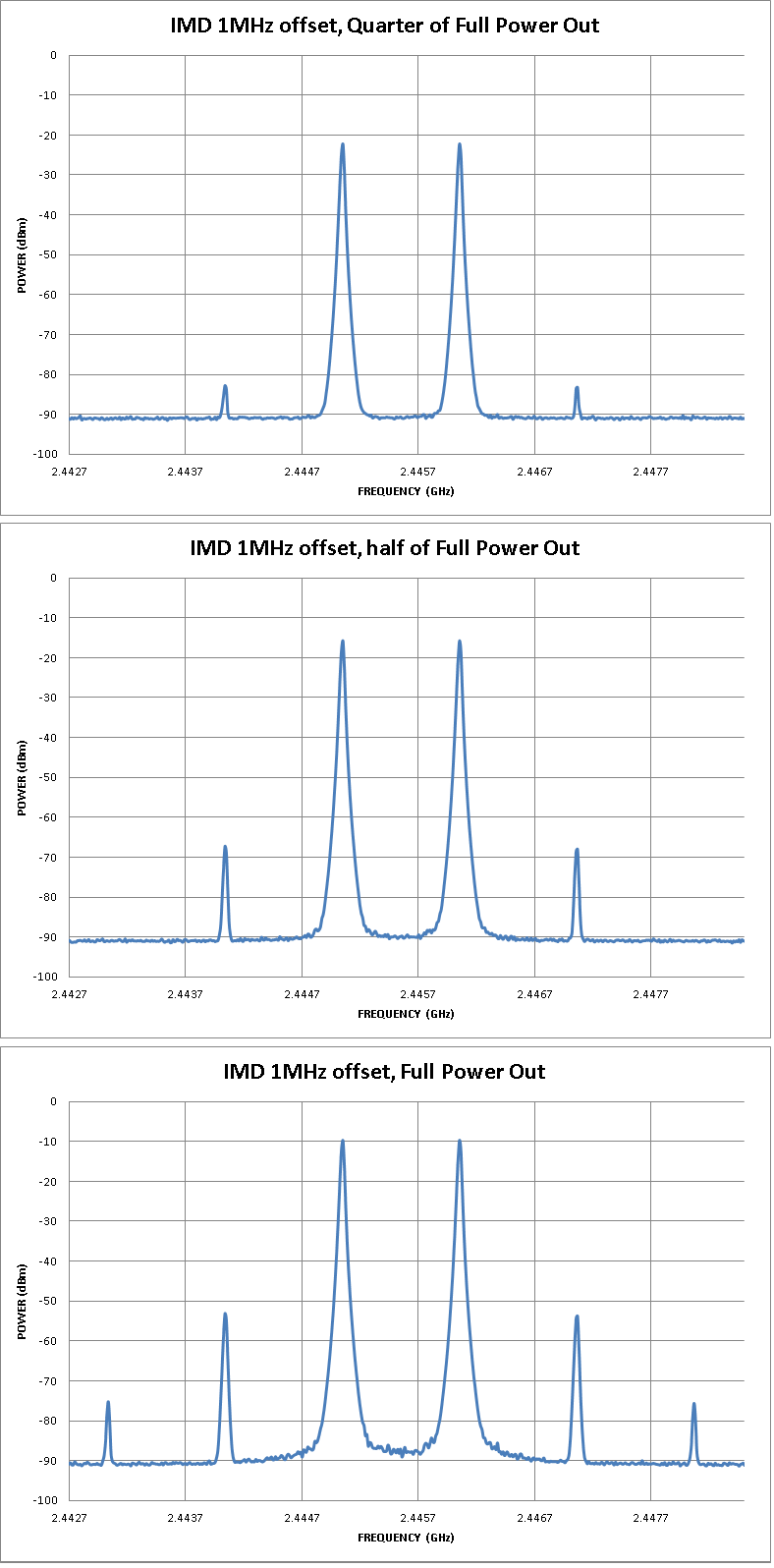
1MHz Offset, LO 1.2GHz, 0dBm input |
1MHz Offset, LO 1.2GHz, -6dBm input |
1MHz Offset, LO 1.2GHz, -12dBm input |
|
|
|
1MHz Offset, LO 2.4GHz, 0dBm input |
1MHz Offset, LO 2.4GHz, -6dBm input |
1MHz Offset, LO 2.4GHz, -12dBm input |
|
|
|
1MHz Offset, LO 3.6GHz, 0dBm input |
1MHz Offset, LO 3.6GHz, -6dBm input |
1MHz Offset, LO 3.6GHz, -12dBm input |


Bandwidth (Modified Board)
|
|
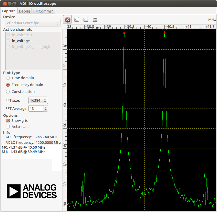
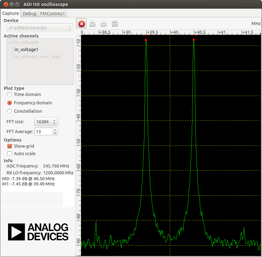
BW with 1.2GHz LO and 0dBm input (Ch1). |
BW with 1.2GHz LO and 0dBm input (Ch2). |


|
|
BW with 2.4GHz LO and 0dBm input (Ch1). |
BW with 2.4GHz LO and 0dBm input (Ch2). |


|
|
BW with 3.6GHz LO and 0dBm input (Ch1). |
BW with 3.6GHz LO and 0dBm input (Ch2). |

