ZCU102 Quick start
This guide provides quick instructions on how to setup the EVAL-AD9656 on:
ZCU102 on FMC HPC0
Using no-OS as software
Necessary files
The following files are needed for the system to boot:
HDL boot file:
system_top.xsano-OS project: projects/ad9656_fmc
Instructions on how to build the boot files from source can be found here:
AD9656_FMC no-OS Example Project. More no-OS build details at No-OS Build Guide.
AD9656-FMC HDL project. More HDL build details at Build an HDL project.
Required software
AMD Xilinx Vivado and Vitis (downloading Vitis from here will include Vivado as well)
An UART terminal (Putty/Tera Term/Minicom, etc.), Baud rate 115200 (8N1)
Required hardware
AMD Xilinx ZCU102 Rev 1.0 FPGA board and its power supply
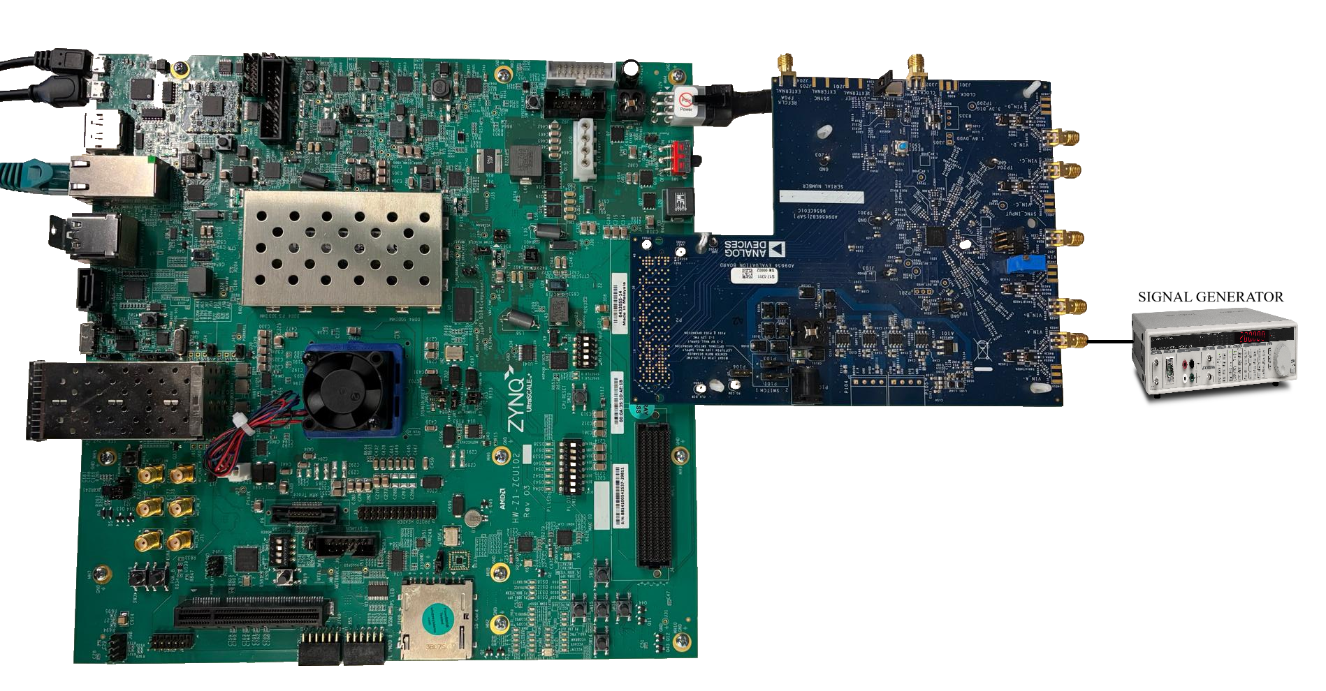
EVAL-AD9656 FMC evaluation board
2x Micro-USB cables, one for UART and one for JTAG
Signal generator
More details as to why you need these, can be found at Prerequisites.
Testing
Creating the setup
All the products described on this page include ESD (electrostatic discharge) sensitive devices. Electrostatic charges as high as 4000V readily accumulate on the human body or test equipment and can discharge without detection. Although the boards feature ESD protection circuitry, permanent damage may occur on devices subjected to high-energy electrostatic discharges. Therefore, proper ESD precautions are recommended to avoid performance degradation or loss of functionality. This includes removing static charge on external equipment, cables, or antennas before connecting to the device.
Follow the steps in this order, to avoid damaging the components:
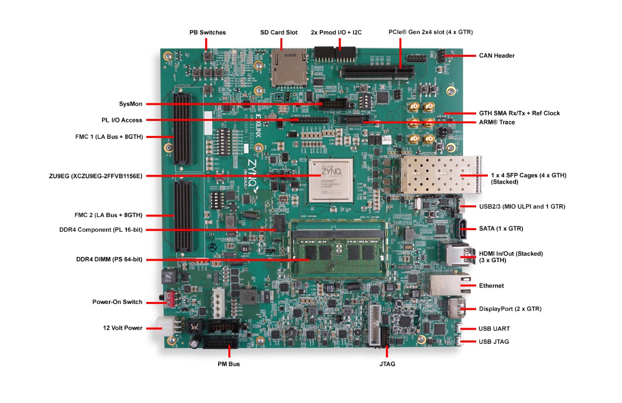
Get the ZCU102.
Configure ZCU102 for JTAG boot mode (mode SW6[4:1] switch in the position ON,ON,ON,ON).
Connect Pin 1 to Pin 2 on both P101 and P103 to power the EVAL-AD9656 through the FMC connector. For other power modes, take a look here.
Connect the EVAL-AD9656 FMC board to the FPGA carrier FMC HPC0 socket (J5).
Connect USB UART (Micro-USB) to your host PC (J83).
Connect USB JTAG (Micro-USB) to your host PC (J2).
Plug the Power Supply into 12V Power input connector (J52).
Turn on the power switch on the FPGA board.
Build and run the project using the steps shown in here.
Observe console output messages on your terminal (use the first ttyUSB or COM port registered).
See also
For more detailed information on ZCU102 switch configuration, check the ZCU102 Hardware User Guide (chapter “MPSoC Device Configuration”) here.
Console output
The following is what is printed in the serial console, after you have connected to the proper ttyUSB or COM port:
Zynq MP First Stage Boot Loader
Release 2023.2   Feb 25 2026  -  08:49:19
PMU-FW is not running, certain applications may not be supported.
The ad9508 chip successfully configured
The ad9553 chip successfully configured
The ad9656 chip successfully configured
ad9656_xcvr: OK (2500000 kHz)
ad9656_jesd status:
        Link is enabled
        Measured Link Clock: 62.498 MHz
        Reported Link Clock: 62.500 MHz
        Lane rate: 2500.000 MHz
        Lane rate / 40: 62.500 MHz
        LMFC rate: 3.906 MHz
        Link status: DATA
        SYSREF captured: disabled
        SYSREF alignment error: disabled
ad9656_adc: Successfully initialized (124996948 Hz)
main ad9656 - PN9 sequence checked!
main ad9656 - PN23 sequence checked!
User input test sequence started!
DMA_EXAMPLE: address=0x800000 samples=32768 channels=4 bits=16
ad9656: setup, configuration and test program is done
Running IIOD server...
If successful, you may connect an IIO client application by:
1. Disconnecting the serial terminal you use to view this message.
2. Connecting the IIO client application using the serial backend configured as shown:
   Baudrate: 115200
   Data size: 8 bits
   Parity: none
   Stop bits: 1
   Flow control: none