HSC-ADC-EVALEZ Quick start
This guide provides quick instructions on how to set up the EVAL-AD9656 with the HSC-ADC-EVALEZ FPGA-based data capture kit using VisualAnalog and SPIController software on a Windows PC.
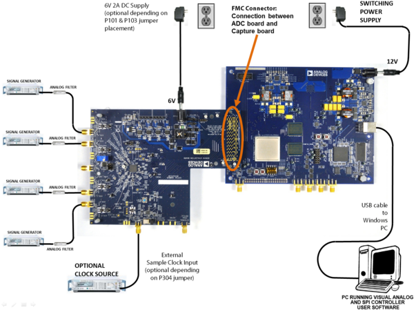
Figure 1 Evaluation Board Connection — EVAL-AD9656 (on Left) and HSC-ADC-EVALEZ (on Right)
Equipment needed
Analog signal source(s) and antialiasing filter(s)
Sample clock source (if not using the on-board crystal oscillator)
Switching power supply (6.0V, 2.5A) for AD9656EBZ
Switching power supply (12V, 3.3A) for HSC-ADC-EVALEZ
PC running Windows
USB 2.0 port
EVAL-AD9656 board
HSC-ADC-EVALEZ FPGA-based data capture kit
Required software
Install the following software on the PC before proceeding:
Configuring the board
Before using the software for testing, configure the evaluation board as follows:
Connect the EVAL-AD9656 to the HSC-ADC-EVALEZ data capture board.
Confirm that the jumpers are installed as shown in the user guide.
The EVAL-AD9656 can be powered in one of three ways. The default is to have the board obtain its power from the HSC-ADC-EVALEZ through the FMC connector. For this configuration, jumper Pin 1 to Pin 2 on both P101 and P103. The other power configurations are described in the user guide.
Connect the 12V, 3.3A switching power supply to the HSC-ADC-EVALEZ board.
Connect the HSC-ADC-EVALEZ board (P702) to the PC using a USB cable.
On the ADC evaluation board, use a clean signal generator with low phase noise to provide an input signal to the desired channel(s). Use a shielded, RG-58, 50Ω coaxial cable (optimally 1 m or shorter) to connect the signal generator. For best results, use a narrow-band, band-pass filter with 50Ω terminations and an appropriate center frequency.
Setting up the ADC data capture
After configuring the board hardware, set up the ADC data capture using the following steps:
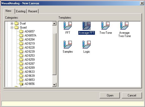
Start VisualAnalog on the connected PC. The appropriate part type should be listed in the status bar of the VisualAnalog — New Canvas window. Select the template that corresponds to the type of testing to be performed (see Figure 2). Average FFT is a good test to start with.
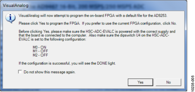
After the template is selected, a message might appear asking if the default configuration can be used to program the FPGA (see Figure 3). If this message appears, click Yes, and the window will close.
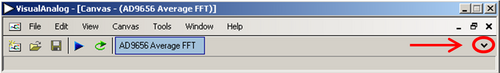
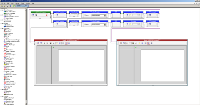
To view the canvas and associated functional blocks, click the Expand Display button, located on the bottom right corner of the window (see Figure 4), to see what is shown in Figure 5.
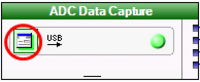
To configure VisualAnalog to operate with the AD9656, push the Settings button on the ADCDataCapture block, as shown in Figure 6.
In the ADC Data Capture Settings Window, General Tab, select AD9656 to be the device, enter the sample clock frequency (125 is the default value), as shown in Figure 7. The sample frequency entered here is used for scaling of frequency values in test results and graphs. In the Output Data field, the channels to be tested are selected, as well as the FFT capture depth (“Length”). Note that the total of the capture depths for all selected channels cannot exceed 256k.
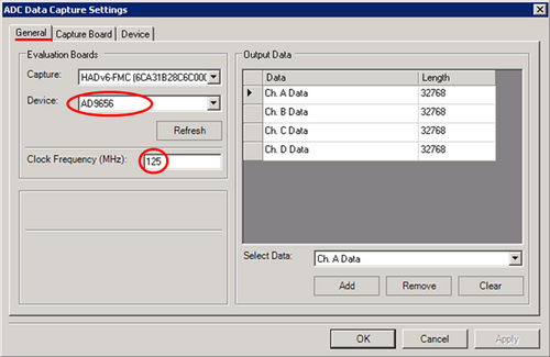
Figure 7 VisualAnalog ADC Data Capture Settings Window, General Tab
In the ADC Data Capture Settings Window, Capture Board Tab, enter 60 in the Fill Delay field. Push the Browse button to navigate to the FPGA program file for the AD9656. The default installation location and filename will be similar to:
C:\Program Files\Analog Devices\VisualAnalog\Hardware\HADv6\AD9656_hadv6fmc.mcs. Push the program button.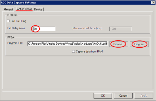
Figure 8 VisualAnalog ADC Data Capture Settings Window, Capture Board Tab
In the ADC Data Capture Settings Window, Device Tab, check the Enable Data Capture Controls checkbox. The capture control fields will be enabled. Select:
GTX RX Equalization: 6
Encode: 125MSPS (default configuration)
Number of lanes: 2 Lanes (At least 2 lanes are required for 125MSPS. The single lane bitrate at 125MSPS would exceed the driver and FPGA capabilities.)
Leave the other checkboxes unchecked.
Though the AD9656 supports a wide variety of converter/lane/sample rate configurations, the software supports only the configurations in the software menu as an out-of-the-box functional kit. If other sample rates or configurations are required, an additional external clock is likely needed.
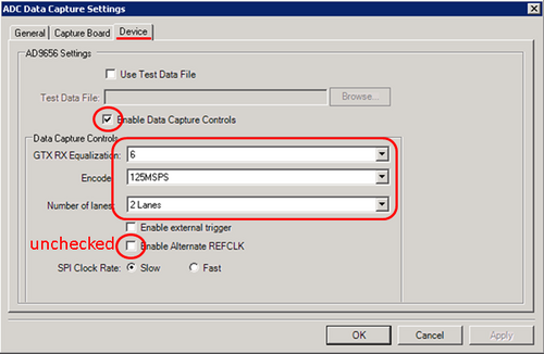
Figure 9 VisualAnalog ADC Data Capture Settings Window, Device Tab
VisualAnalog is now set up to work with the AD9656EBZ in the default configuration. Other VisualAnalog features and capture settings are documented in the AN-905 Application Note, VisualAnalog Converter Evaluation Tool Version 1.0 User Manual.
Setting up the SPI Controller software
After the ADC data capture board setup is complete, set up the SPI controller software using the following procedure:
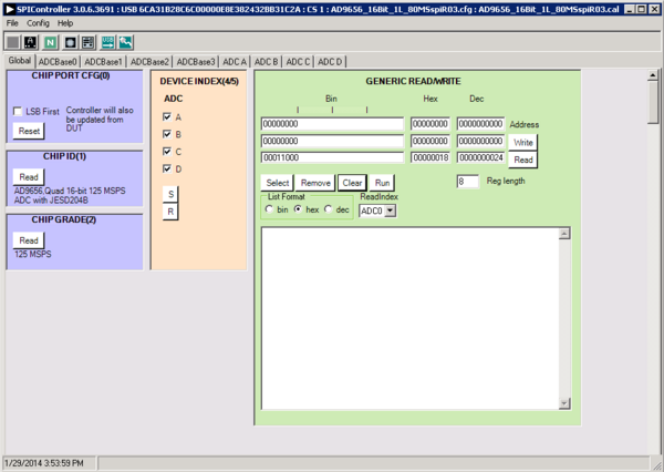
Open the SPI controller software by going to the Start menu or by double-clicking the SPIController software desktop icon. If prompted for a configuration file, select the .cfg file whose name begins with AD9656. If not prompted, check the title bar of the window to determine which configuration is loaded. If necessary, choose Cfg Open from the File menu and select the appropriate file based on your part type. Note that the CHIP ID(1) box should be filled to indicate whether the correct SPI controller configuration file is loaded (see Figure 10).
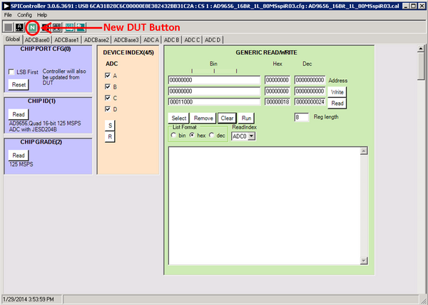
Click the New DUT button in the SPIController window (see Figure 11).
In the ADCBase0 tab of the SPIController window, find the CLOCK DIVIDE(B) box (see Figure 12), and the MODES(8) box (see Figure 13). If using the clock divider, use the drop-down box to select the correct clock divide ratio, if necessary. If there is any interruption of the ADC clock during power-up or during operation, a Digital Reset may be needed to re-initialize the ADC (Figure 13). For additional information, refer to the data sheet, the AN-878 Application Note, High Speed ADC SPI Control Software, and the AN-877 Application Note, Interfacing to High Speed ADCs via SPI.
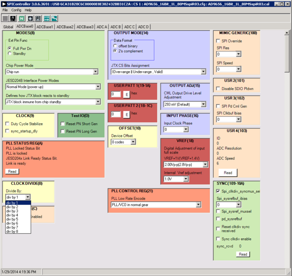
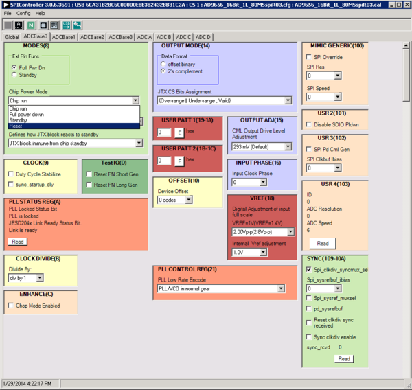
Figure 13 SPI Controller, Chip Power Mode - Digital Reset Selection
In the ADCBase1 tab of the SPIController window, set the number of lanes the AD9656 will be configured to. Note that the number of lanes selected here must match the settings made in VisualAnalog as shown in Step 7, Figure 9 above.
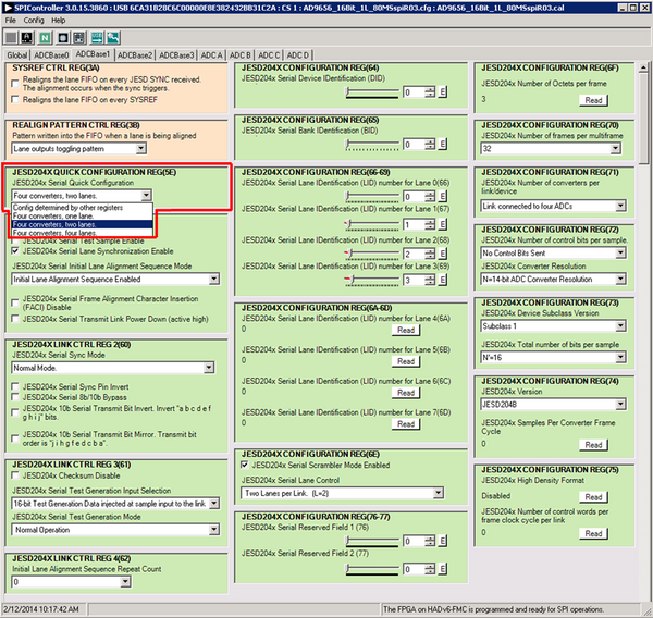
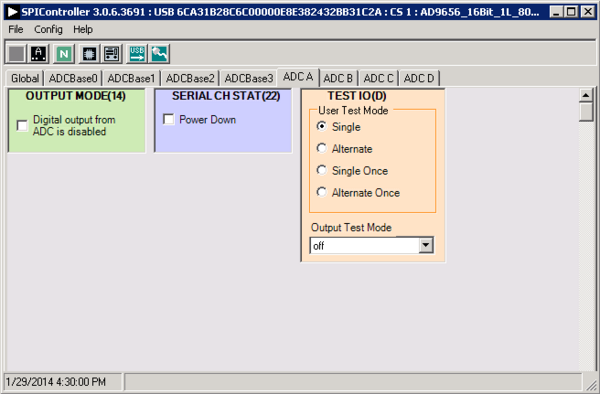
Note that other settings can be changed on the ADCBase0 tab (see Figure 12) and the ADC A through ADC D tabs (see Figure 15) to set up the part in the desired mode. The ADCBase0 tab settings affect the entire part, whereas the settings on the ADC A through ADC D tabs each affect the selected channel only. See the data sheet, the AN-878 Application Note, High Speed ADC SPI Control Software, and the AN-877 Application Note, Interfacing to High Speed ADCs via SPI, for additional information on the available settings.
Invoke a Digital Reset as shown in Figure 13 before testing. After selecting Reset, select Chip Run to return to normal operation.
To begin testing, click the Run or Continuous Run button in the VisualAnalog toolbar (see Figure 16).
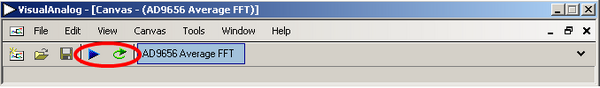
Figure 16 Run/Continuous Run Buttons (Encircled in Red) in VisualAnalog Toolbar, Collapsed Display
Adjusting the amplitude of the input signal
Adjust the amplitude of the input signal for each channel as follows:
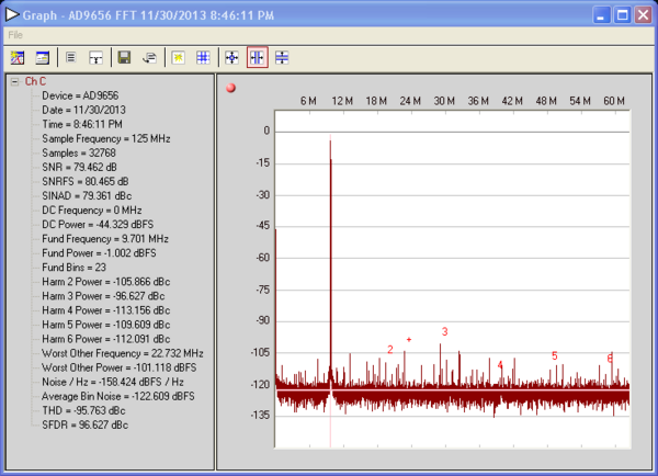
Adjust the amplitude of the input signal so that the fundamental is at the desired level. Examine the Fund Power reading in the left panel of the VisualAnalog Graph - AD9656 FFT window (see Figure 17).
Repeat this procedure for the other channels, if desired.
Click the floppy-disk icon within the VisualAnalog Graph - AD9656 FFT window to save the performance data as a .csv formatted file for plotting or analysis.
Troubleshooting
Lack of SPI communication will cause difficulty in configuring the ADC.
Go to the Global tab of the SPIController window and push the Read button in the GENERIC READ/WRITE window. This will read the contents of ADC register 0x00. If SPI communication is working properly and the ADC is powered up, the value 0x18 hexadecimal will appear. If the contents show 0x00, the ADC is not powered up or SPI communication is not working.
Check that there is correct power to the EVAL-AD9656 board, and to the HSC-ADC-EVALEZ.
Check that the USB cable is properly connected from the PC to the HSC-ADC-EVALEZ.
The LED on the VisualAnalog ADCDataCapture block should be green. If it is red, push the USB button on the same block to refresh the connection.
If the FFT plot appears abnormal, do the following:
If you see an abnormal noise floor, go to the ADCBase0 tab of the SPIController window and toggle the Chip Power Mode in MODES(8) from Chip Run to Reset and back (Figure 13).
If you see a normal noise floor when you disconnect the signal generator from the analog input, be sure that you are not overdriving the ADC. Reduce the input level, if necessary.
In VisualAnalog, click the Settings icon in the Input Formatter block. Check that Number Format is set to the correct encoding (twos complement by default). Check that the Number Format in the VisualAnalog Input Formatter matches the data format selected in the SPIController ADCBase0 OUTPUT MODE(14) window. Repeat for the other channels.
If the FFT appears normal but the performance is poor, check the following:
Make sure that an appropriate filter is used on the analog input.
Make sure that the signal generators for the clock and the analog input are clean (low phase noise).
Change the analog input frequency slightly if noncoherent sampling is being used.
Make sure that the SPI configuration file matches the product being evaluated.
If the FFT window remains blank after Run in VisualAnalog (see Figure 16) is clicked, do the following:
Make sure that the evaluation board is securely connected to the HSC-ADC-EVALEZ board.
Make sure that the correct FPGA program was installed by clicking the Settings icon in the ADC Data Capture block in VisualAnalog. Then select the FPGA tab and verify that the proper FPGA .mcs file (one containing “AD9656” in the filename) is selected for the part.
Make sure that the FPGA has been programmed by verifying that the CONFIG_DONE LED is illuminated on the HSC-ADC-EVALEZ board. If the CONFIG_DONE LED is not illuminated, click the Settings icon in the ADC Data Capture block in VisualAnalog. Then select the FPGA tab and verify that the proper FPGA .mcs file (one containing “AD9656” in the filename) is selected for the part. Then push the Program button. The LED should light up.
On the EVAL-AD9656 there is an LED next to a reset button (S501). If this LED is not lit, push the reset button and try running again.
Helpful documents
AD9656 data sheet
High speed ADC FIFO evaluation kit (HSC-ADC-EVALEZ)
HSC-ADC-EVALEZ Wiki Guide hsc-adc-evale
AN-905 Application Note, VisualAnalog Converter Evaluation Tool Version 1.0 User Manual
AN-878 Application Note, High Speed ADC SPI Control Software
AN-877 Application Note, Interfacing to High Speed ADCs via SPI
AN-835 Application Note, Understanding ADC Testing and Evaluation