AD-FMCOMMS1-EBZ Quick Start Guide on Xilinx FPGA Boards Without OS
Warning
Analog Devices uses six designations to inform our customers where a semiconductor product is in its life cycle. From emerging innovations to products which have been in production for twenty years, we understand that insight into life cycle status is important. Device life cycles are tracked on their individual product pages on analog.com, and should always be consulted before making any design decisions.
This particular article/document/design has been retired or deprecated, which means it is no longer maintained or actively updated, even though the devices themselves may be Recommended for New Designs or in Production. This page is here for historical/reference purposes only.
This guide provides some quick instructions on how to setup the AD-FMCOMMS1-EBZ on either:
Important
The ML605 XPS project remain on this website only for legacy purposes. The support for XPS projects has been discontinued.
Required Software
The supported Xilinx tools version for each release can be found on the HDL releases page.
Required Hardware
AD-FMCOMMS1-EBZ FMC Board
- Xilinx ML605 / Xilinx AC701 / Xilinx KC705 / Xilinx VC707 / Xilinx ZC702 /
Xilinx ZC706 / Digilent ZED
Downloads
Download
no-OS Drivers (last supported release): fmcomms1
ML605 HDL Reference Design for ISE: cf_xcomm
HDL Reference Design for Vivado 2015.4 (last supported release): projects/fmcomms1
Hardware Setup
Connect the power and UART cables of the Xilinx FPGA board
Connect the AD-FMCOMMS1-EBZ FMC board to the Xilinx FPGA board on the:
LPC FMC connector for KC705, ZC706, ZED;
LPC FMC1 connector for ZC702;
HPC FMC connector for AC701, ML605;
HPC FMC2 connector for VC707.
The transmit signal may be observed using a spectrum analyzer. The receive side may be sourced by either the transmit side or a signal source. If it is the transmit side, connect an SMA cable from the transmit to receive or connect antennae on both. If it is a signal source the frequency needs to be 2.4G+f, 0 dBm where f is the baseband.
Note
The default RX gain in case of no-OS software is 10 dB. This could be too high, when an SMA cable is used for external loop-back. In this case the user should reduce the RX gain to its minimum value: 4.5 dB, in order to prevent saturation.
Software Setup for Vivado
Example for a ZC702 board:
After building the project in Vivado for the used FPGA board, a SDK_Export folder will be created in ../fmcomms1_board.sdk/SDK
Open the Xilinx SDK for Vivado. When the SDK starts it asks to provide a folder where to store the workspace. Any folder can be provided.
Go to File->New->Application project
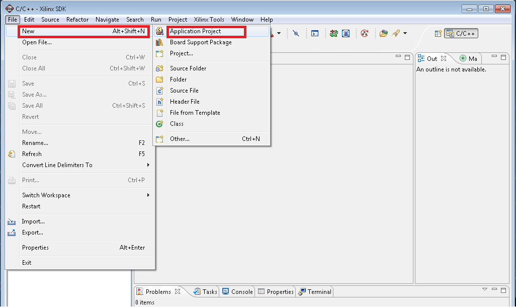
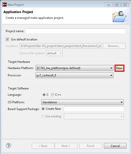
Use a new hardware platform, so choose New in Target Hardware section
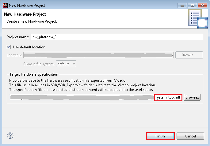
At the Target Hardware Specification section browse the location of the hardware description file. This file’s extension should be .xml or .hdf, and is located in the directory of the hdl design. Note: If the file does not exist, probably you forgot to make an Export hardware (in Vivado File -> Export -> Export Hardware…)
Then give a name to the project and click Next
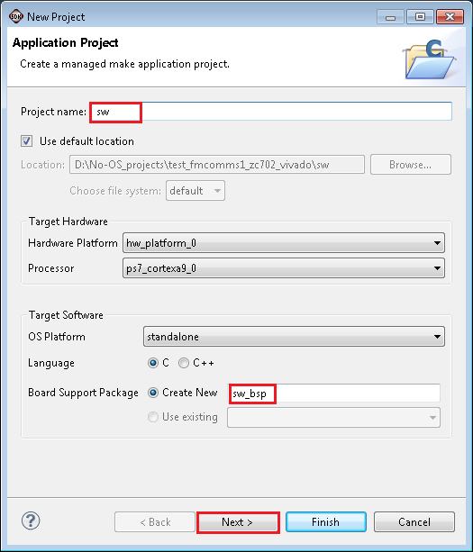
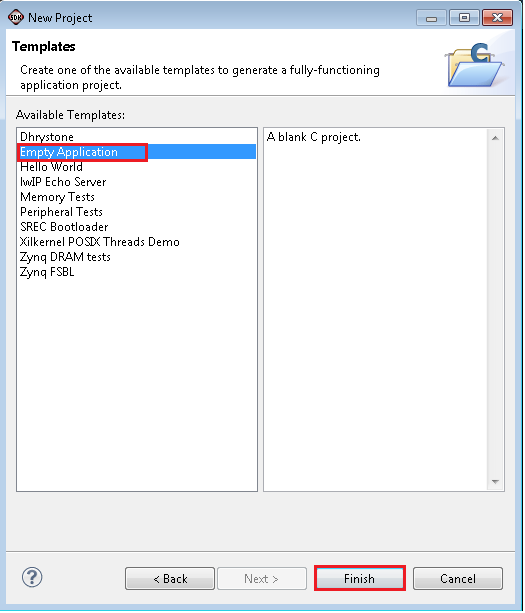
In the next window choose Empty Application and click Finish
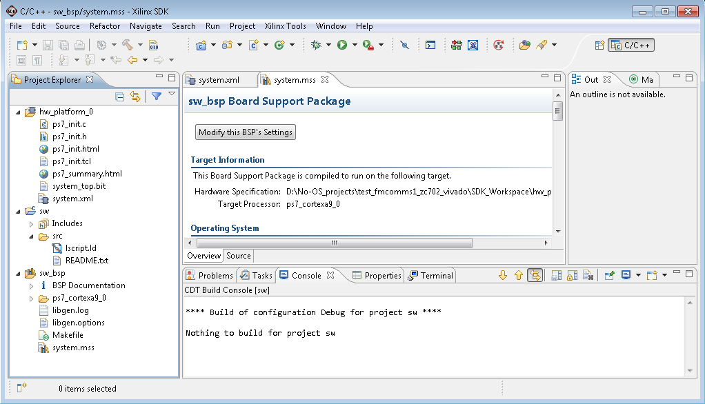
Now the project without source code looks like this
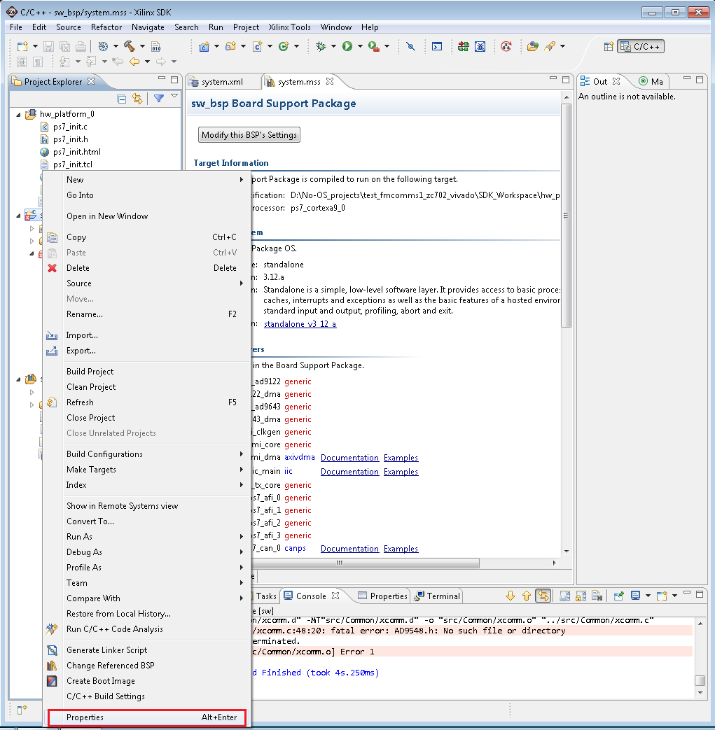
Then the source code(all folders from no-OS Drivers, except Chipscope, Evaluate and PIC) must be added from Github to src folder.

Afterwards click right on project name and go to Properties
In the window that appears go to Settings->Directories and include the paths of the directories from src for both Debug and Release configurations.

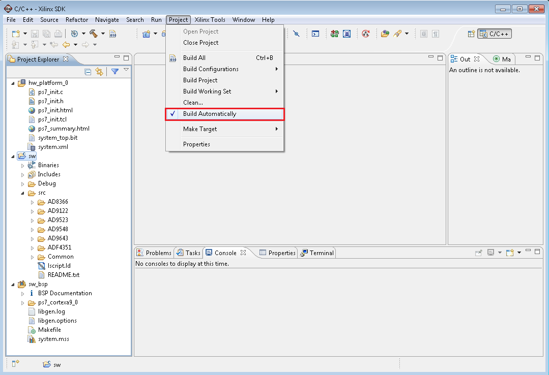
The Project Explorer window now shows the projects that exist in the workspace and the files for each project. The SDK should automatically build the projects and the Console window will display the result of the build. If the build is not done automatically select the Project->Build Automatically menu option.
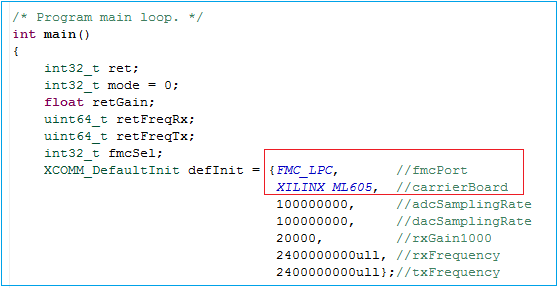
The default project configuration assumes that a Xilinx ML605 FPGA board is used and that the FMCOMMS1 is connected to this board on the FMC LPC connector. In the file Common/main.c change the XCOMM_DefaultInit initialization structure so that the FPGA board and the FMC port used to connect the FMCOMMS1 to the FPGA board correspond to your actual hardware setup.
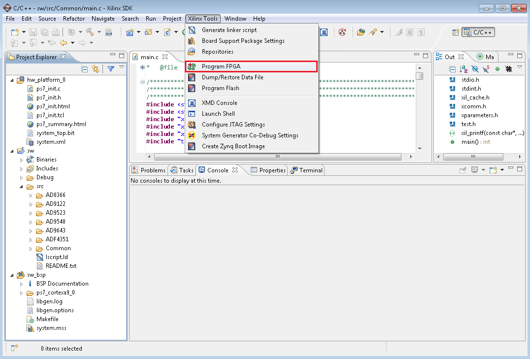
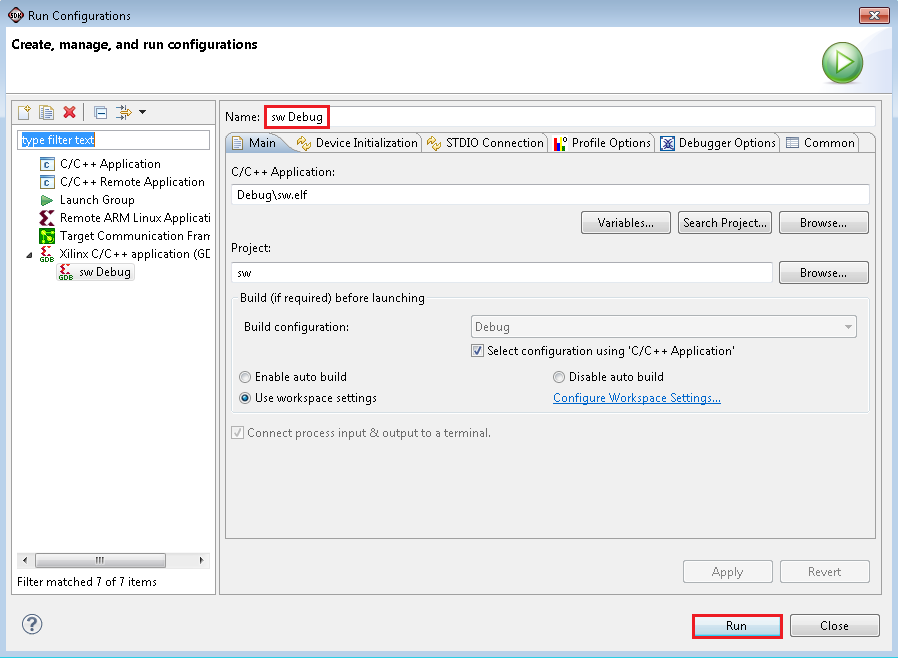
At this point the software project setup is complete, the FPGA can be programmed and the software can be downloaded into the system. You can program the FPGA by going to Xilinx Tools.
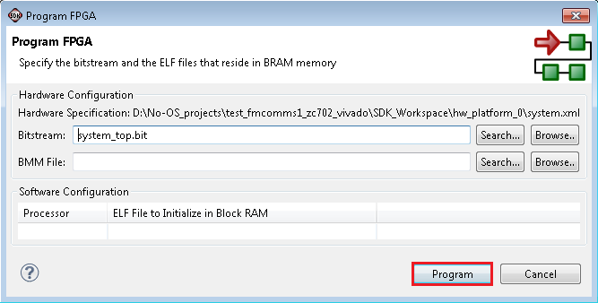
Then choose this bitstream and press Program.
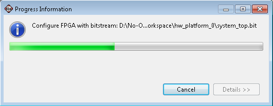
This window will appear next.
Afterwards a Run Configuration must be created and then press Run.
The no-OS drivers source code contains an example on how to:
initialize the board
test the ADC communication
test the DAC communication
set the VGA gain
set the receive and transmit frequencies
send a sinewave over the air and receive it back
The example code outputs on the UART the status of each operation as shown below.
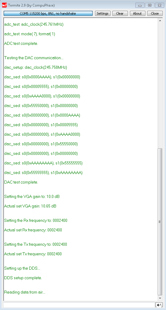
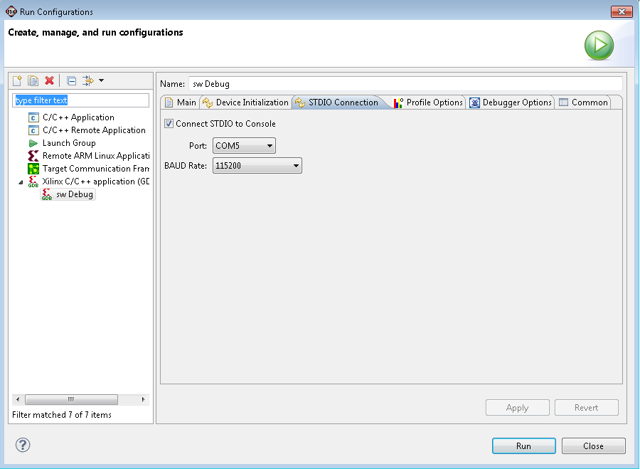
The output of the example program can be viewed in the SDK console by enabling the Connect STDIO Console option and setting the baud rate of the UART port to 115200.
As an alternative an UART terminal can be used to capture the output of the example program. The number of used UART port depends on the computer’s configuration. The following settings must be used in the UART terminal:
Baud Rate: 115200bps
Data: 8 bit
Parity: None
Stop bits: 1 bit
Flow Control: none
The example code is located in the “Common/main.c” file and the implementations of the ADC and DAC test routines can be found in the “Common/test.c” file.
After running the example program the system is configured to generate a sinewave and send it over the air using a 2.4GHz carrier. The signal is received back, brought to baseband again and digitized by the ADC on the FMCOMMS1. The I and Q samples generated by the ADC can be viewed using the Vivado Hardware Manager. These are the steps than need to be followed to view the sine waves:
First make sure that the board is programmed and the program is currently running
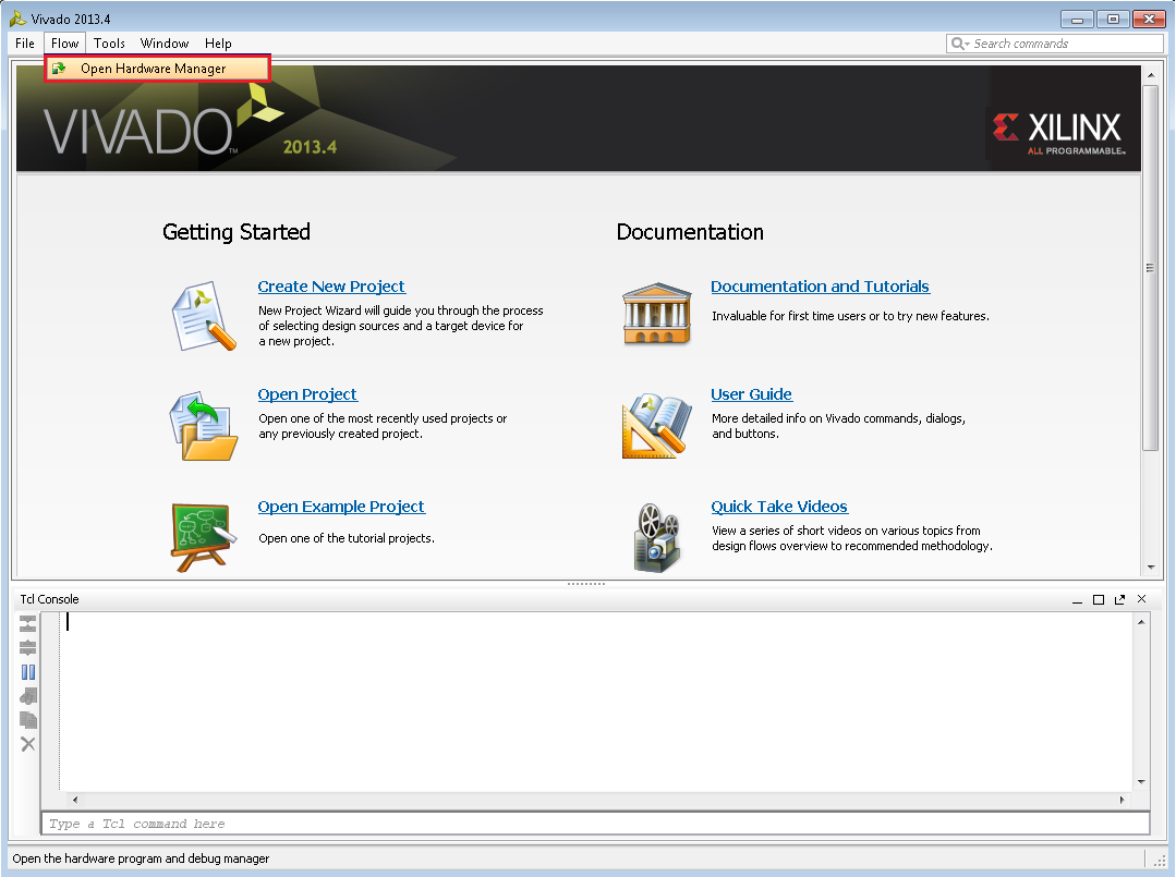
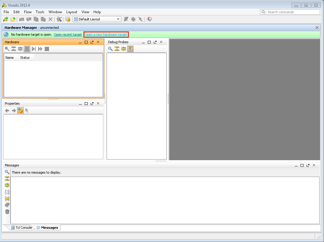
Then open Vivado and go to Flow->Open Hardware manager
In the new window select Open a new hardware target
Then click Next 4 times and then Finish


This is how the Vivado Hardware Manager looks like. Now go to Probes files.
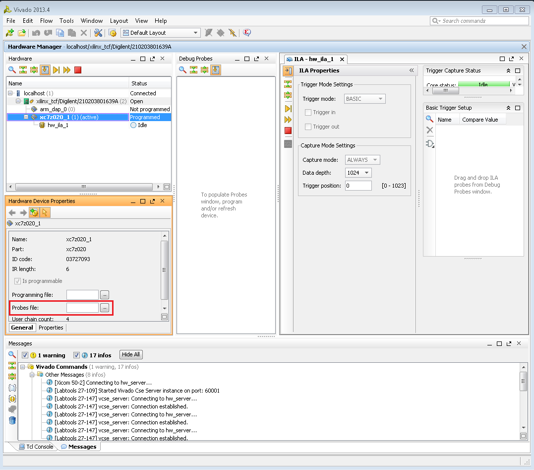
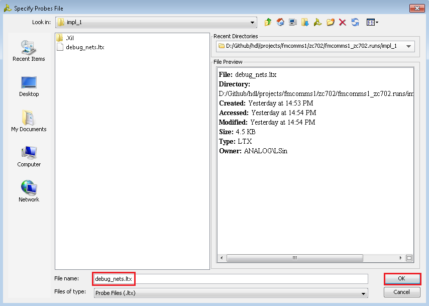
And browse for the folder where the project was compiled ../fmcomms1_board.runs/impl_1/debug_nets.ltx
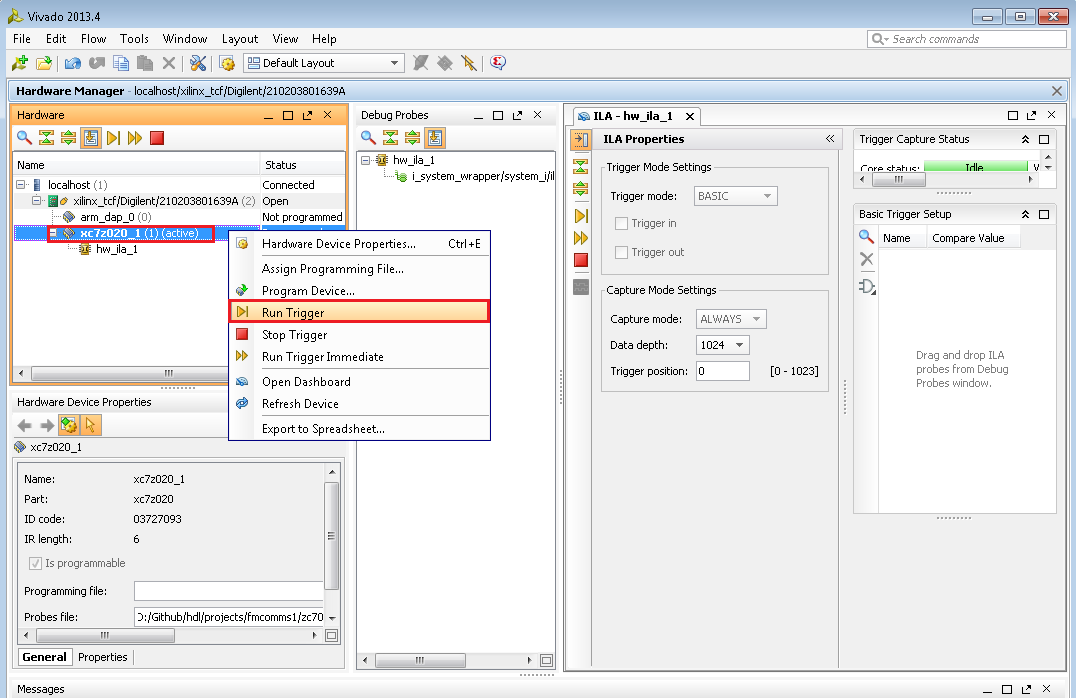
Then do a right click on the active target and choose Refresh Device
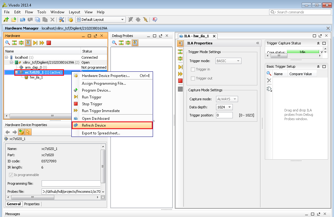
Afterwards do another right click on the active target and choose Run Trigger
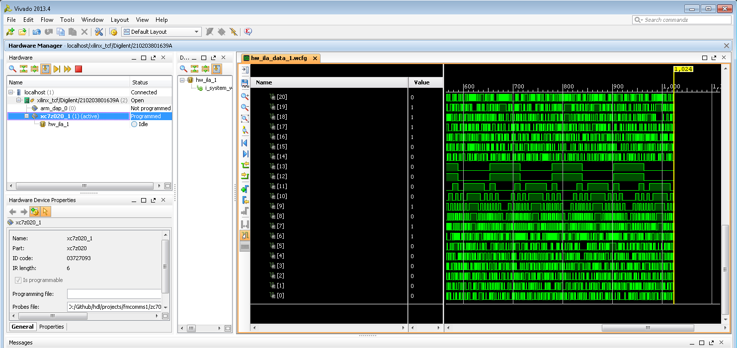
- This is how the 56 digital signals look like. Now we have to compose the
sinewaves.
First select the first 14 signals, do a right click and choose New Virtual Bus

Then give a name to that virtual bus

In order to see a sinewave you have to right click on the name of the virtual bus, choose Analog for Waveform Style option.

Now you can see a sinewave, but the radix is not the good one. In order to have the right radix, you must choose Signed Decimal for Radix.

Now the signal looks like a sinewave

And after you did the same steps for the other 3x14 remaining signals, you should have 4 sinewaves composed of 56 signals. Because of the working frequency of the ILA core, data has been split into 2 buses, so the actual data from the Evaluation board would be I_0 interleaved with I_1, and Q_0 interleaved with Q_1.
