Evaluating the AD9208 / AD9689 / AD9699 Analog-to-Digital Converter
Overview
The evaluation board design is shared between the following device variants: AD9208 / AD9689 / AD9699.
This user guide describes the AD9208-3000EBZ, AD9689-2600EBZ and AD9689-2000EBZ evaluation boards which provide all of the support circuitry required to operate the ADC in its various modes and configurations. This guide entails both the hardware and software setup needed to acquire data capture from the evaluation board.
Note
For evaluating AD9699, use only ADS8-V1EBZ and AD9208-3000EBZ channel A input.
There are two FPGA-based data capture boards that can be used to capture data from the AD9208-3000EBZ, AD9689-2600EBZ and AD9689-2000EBZ evaluation boards. The available FPGA boards are ADS7-V2EBZ and ADS8-V1EBZ. The selection of the FPGA board is based on the maximum line rate required in the evaluation. If the line rate needed in the evaluation is <=12.5 Gbps/lane, the ADS7-V2EBZ can be used for data capture. All applications where the line rate required exceeds 12.5 Gbps/lane but is <=16 Gbps/lane will require the ADS8-V1EBZ as the data capture board.
Documents and software tools, where available, can be found at the HS-ADC Eval Board homepage.
For additional information or questions, post a question on EngineerZone, or send an email to highspeed.converters@analog.com.
FPGA board selection
The selection table for the FPGA evaluation board is shown below. Only Full BW modes are shown here. However, this table provides a blueprint for FPGA board selection based on the end application’s JESD204B line rate.
Evaluation Board Part Number |
Sample Rate |
L.M.F Configuration |
JESD204B Line Rate (Gbps/lane) |
Recommended FPGA Data Capture Board |
|---|---|---|---|---|
AD9208-3000EBZ |
3.0 GSPS |
8.2.1 |
15 |
|
AD9208-3000EBZ |
3.0 GSPS |
8.1.1 |
7.5 |
|
AD9689-2600EBZ |
2.6 GSPS |
8.2.1 |
13 |
|
AD9689-2600EBZ |
2.5 GSPS |
8.2.1 |
12.5 |
|
AD9689-2000EBZ |
2.0 GSPS |
8.2.1 |
10 |
This user guide applies to the following evaluation boards:
Evaluation Board Part Number |
Description |
Board Revision |
|---|---|---|
AD9208-3000EBZ |
Evaluation board for AD9208-3000 / AD9699-3000 |
9689CE02C |
AD9689-2600EBZ |
Evaluation board for AD9689-2600 |
9689CE02C |
AD9689-2000EBZ |
Evaluation board for AD9689-2000 |
9689CE02C |
Note
The FPGA image in ADS8-V1EBZ does not support lane rates below 2 Gbps. Hence, the following modes will not give a valid FFT. All modes listed below use a 3 GHz sample clock.
LMF=411 and LMF=412 for a decimation ratio of 8
LMF=811 and LMF=812 for a decimation ratio of 4
LMF=421 and LMF=422 for a decimation ratio of 16
LMF=821 and LMF=822 for a decimation ratio of 8
LMF=442 and LMF=444 for a decimation ratio of 30
LMF=841 and LMF=842 for decimation ratios of 15 and 16
Features
Full featured evaluation board for the AD9208 / AD9689 / AD9699
JESD204B coded serial digital outputs with support for lane rates up to 16 Gbps/lane
Wide full power bandwidth supports IF sampling of signals up to 9 GHz (-3 dB point)
Four integrated wide-band decimation filter and NCO blocks supporting multi-band receivers
Fast NCO switching enabled through GPIO pins
Flexible SPI interface controls various product features and functions
Programmable fast over range detection and signal monitoring
On-chip temperature diode for system thermal management
Helpful documents
AN-905 Application Note, VisualAnalog Converter Evaluation Tool Version 1.0 User Manual
AN-835 Application Note, Understanding ADC Testing and Evaluation
Software needed
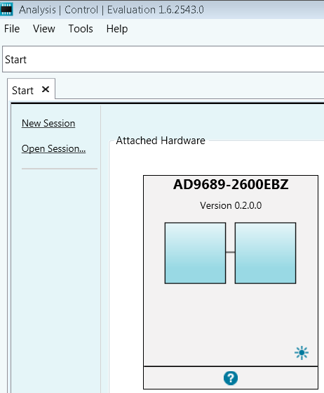
ACE (Analysis| Control| Evaluation)
Design and integration files
Note
The AD9208-3000EBZ, AD9689-2600EBZ and the AD9689-2000EBZ use the same design files. The only difference is in the ADC choice.
Equipment needed
PC running Windows
USB 2.0 port and USB 2.0 High-speed A to B Cable
AD9208-3000EBZ / AD9689-2600EBZ / AD9689-2000EBZ evaluation board
ADS7-V2EBZ or ADS8-V1EBZ FPGA-based data capture kit
12V, 6.5A switching power supply (such as the SL POWER CENB1080A1251F01 supplied with ADS7-V2EBZ)
Low phase noise analog input source and antialiasing filter
Low phase noise sample clock source
Reference clock source
Typical setup
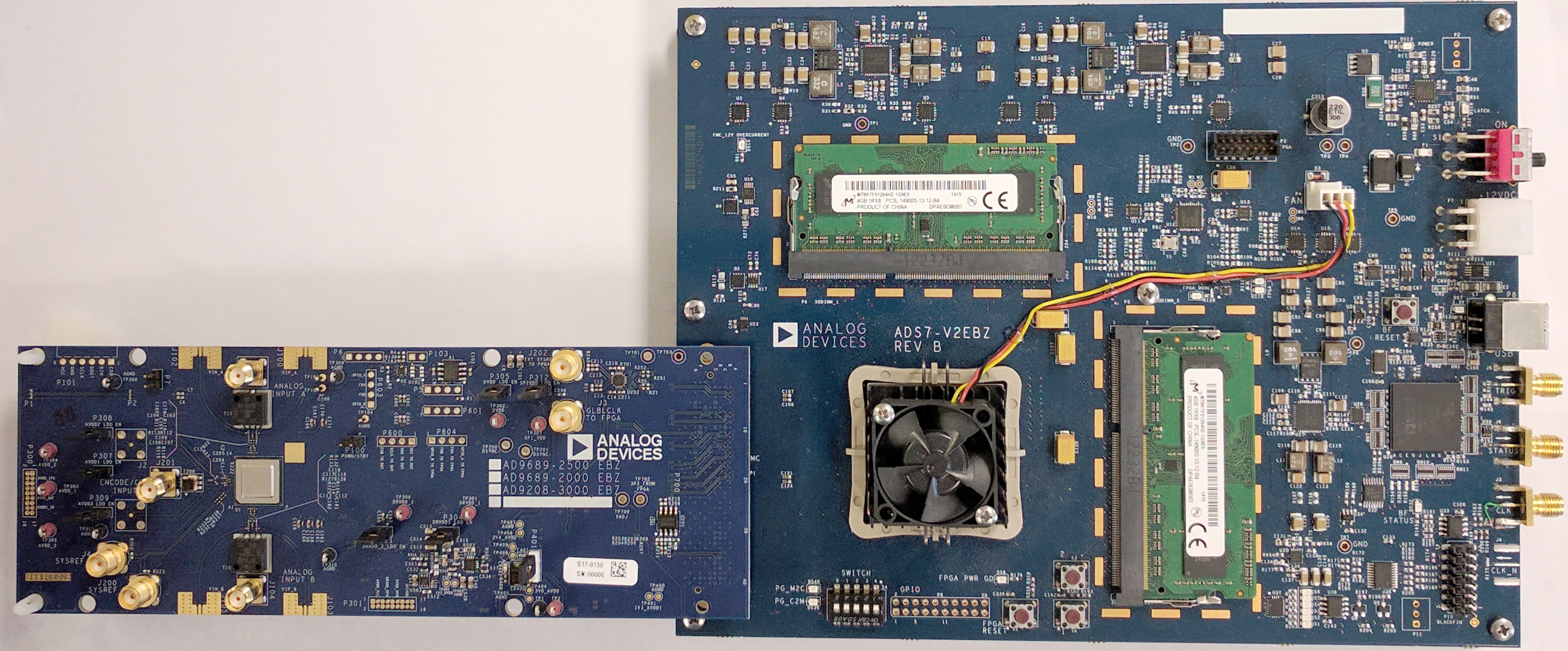
Figure 1 a. AD9208-3000EBZ / AD9689-2600EBZ / AD9689-2000EBZ (Left) and ADS7-V2EBZ (Right)

Figure 1b. AD9208-3000EBZ / AD9689-2600EBZ / AD9689-2000EBZ (Left) and ADS8-V1EBZ (Right)
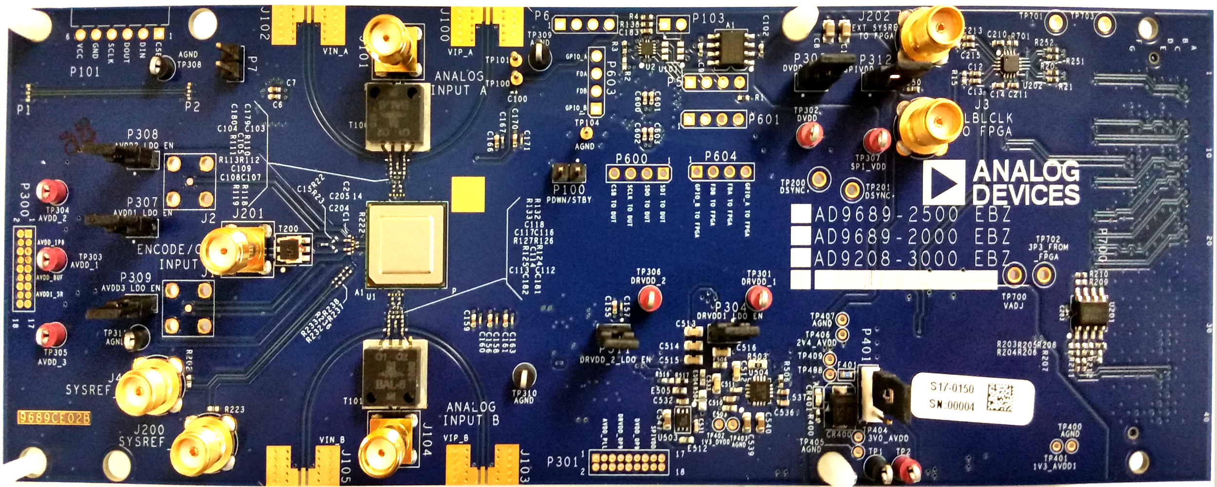
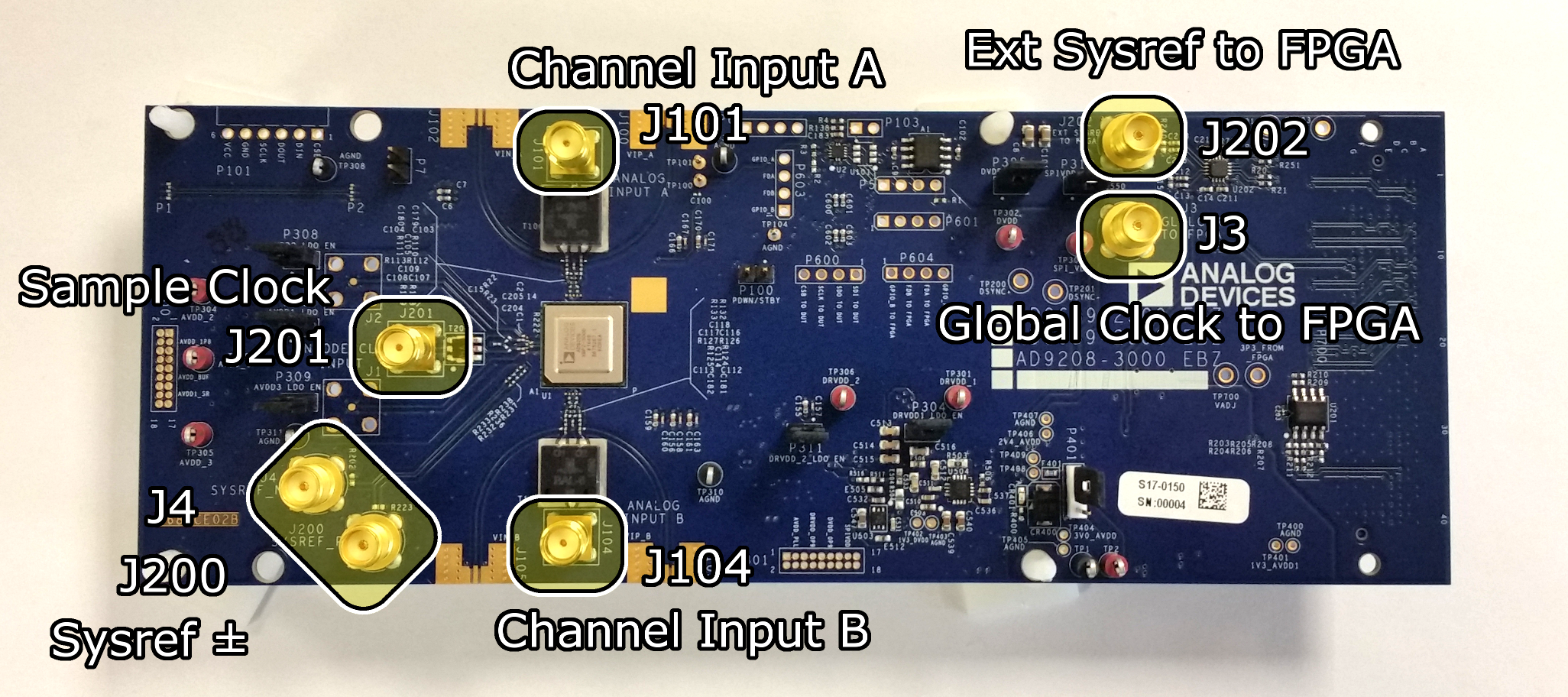
Figure 2 Top-side of AD9208-3000EBZ / AD9689-2600EBZ / AD9689-2000EBZ Board
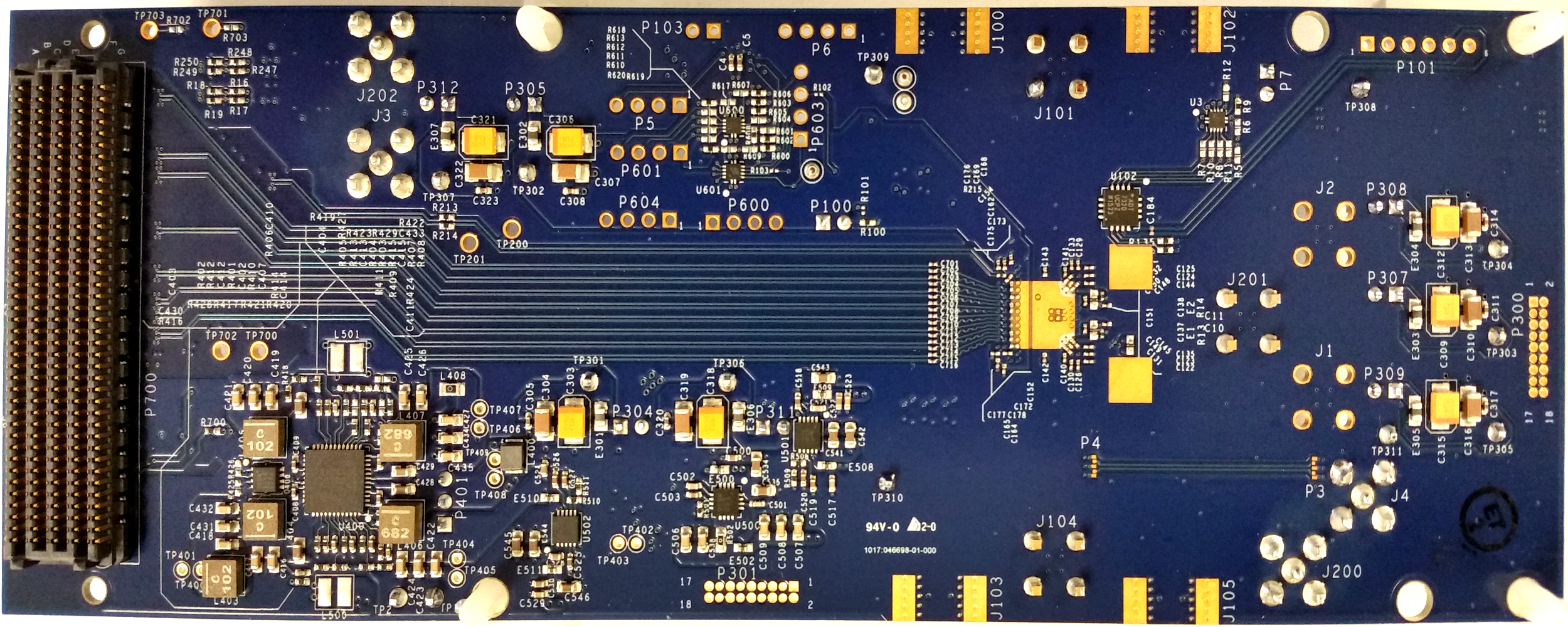
Figure 3 Bottom-side of AD9208-3000EBZ / AD9689-2600EBZ / AD9689-2000EBZ Board
Getting started
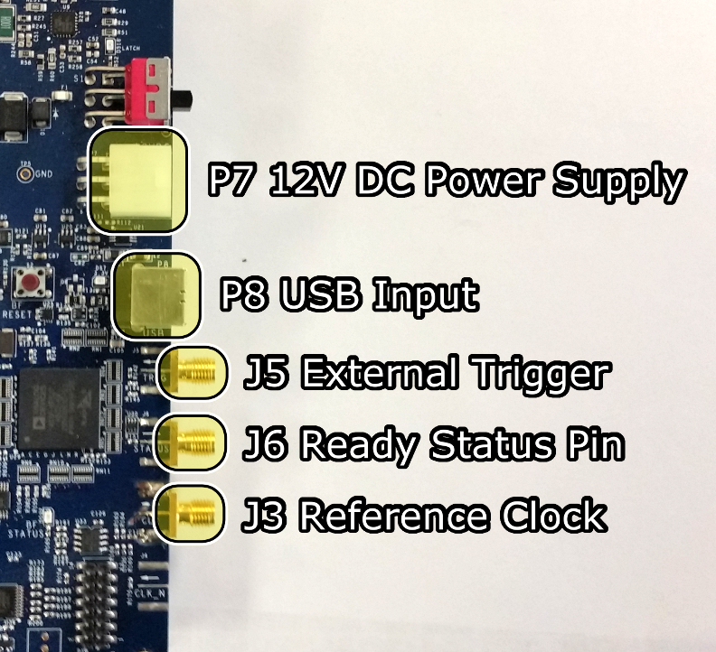
Connector layout
Tip
For more information on SYSREF and Global Clock (J3, J4, J200, J202), see the JESD204B Survival Guide.
Warning
The AD9208-3000EBZ/AD9689-2600EBZ is electrostatic discharge (ESD) sensitive. Handle the device with care, and employ conducting wrist straps or antistatic bags when handling the board.
Configuring the board
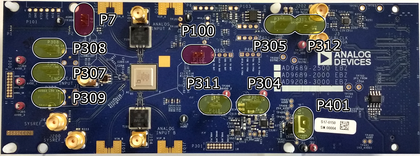
Figure 6 Jumper connections on AD9208-3000EBZ / AD9689-2600EBZ
Before using the software for testing, configure the evaluation boards as follows:
Before connecting the AD9208/AD9689 evaluation board to the ADS7-V2EBZ, jump the following pins: P304, P305, P307, P308, P309, P311, and P312. Do not jump P7 (Temperature Sensor Enable) or P100 (Power Down / Standby). Jump P401 towards the inside of the board, to power the board via FMC. See Figure 6 for all jumper connections.
Ensure that the data capture board is switched to “OFF” (S1 on the data capture board). Connect the evaluation board to the data capture board via the FMC connector found on the underside of the board, as shown in Figure 1. Connect the power supply and USB cable to the data capture board.
Turn on the ADS7-V2EBZ.
The ADS7-V2EBZ should appear in the Device Manager as shown in Figure 7.
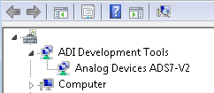
If the Device Manager does not show the ADS7-V2EBZ listed as shown in Figure 7, unplug all USB devices from the PC, uninstall and re-install ACE and restart the hardware setup from step 1.
On the AD9208 evaluation board, provide a clean, low jitter clock source to connector J201 (preferably via a shielded RG-58 50 Ohm coaxial cable) and set the amplitude to 10 dBm. This is the ADC Sample Clock. Set the sample clock frequency to the rated value of 3 GHz for the AD9208 and 2.6 GHz for the AD9689.
On the ADS7-V2EBZ, provide a clean, low jitter clock source to connector J3 and set the amplitude to 10 dBm. This is the Reference Clock for the gigabit transceivers in the FPGA. The REFCLK frequency can be calculated using the following formulae:
\[LaneLineRate = \frac{M \times N' \times \frac{10}{8} \times f_{out}}{L} \times DataPackingRatio \text{ bps/lane}\]where:
\[f_{out} = \frac{f_{ADC\_SAMPLE\_CLOCK}}{DecimationRatio}\]\[N' = 8 \text{ or } 16\]\[REFCLK = \frac{LaneLineRate}{20}\]\[DataPackingRatio = 1 \text{ (default) or } \frac{4}{5} \text{ (for Fsx4 mode)}\]Default N’ = 16; DCM = Chip Decimation Ratio (DCM = 1 for Full Bandwidth Mode); M = Virtual Converters; L = Lanes.
On the AD9208/AD9689 evaluation board, connect a clean signal generator with low phase noise to J101 or J104 via coaxial cable for channels A and B respectively. It is recommended to use a narrow-band, band-pass filter with 50 Ohm terminations and an appropriate center frequency.
ACE setup
Download and install ACE if it is not already installed.
The AD9208 / AD9689 ACE plug-in can be found under the AD9208 Evaluation Board Software Section, AD9689 Evaluation Board Software Section or through ACE’s Plug-In Manager (Tools -> Manage Plug-Ins).
Tip
Some browsers (such as Internet Explorer) may save the file as a .zip file instead of an .acezip file. If this happens, simply download and rename the file with an .acezip file extension.
Once the .acezip file has been downloaded from the Analog Devices website, right click on it and install the plug-in, or double click to install.
Click Start -> All Programs -> Analog Devices -> ACE -> ACE
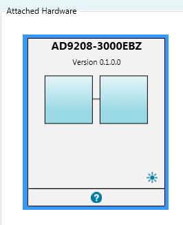
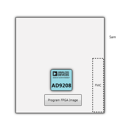
The AD9208/AD9689 plug-in should appear as in Figure 8 if installed properly.
Note
The AD9699 evaluation board shares the same plugin with AD9208.
If the AD9208/AD9689 plug-in does not appear, or no board is detected, make sure the ADS7-V2EBZ is powered on and the evaluation board is properly connected. Make sure that ACE has been updated to the most recent version and the necessary plug-ins have been installed.
Note
Differences may occur between ACE plug-in versions, including the version number seen in Figure 8 above or components in any of the other images below. However, these will not affect the performance of the part nor the fundamental features described in this user guide.
Click on the plug-in to open it. This will open the AD9208/AD9689 Board View. Click the “Program FPGA Image” button to program the ADS7-V2EBZ FPGA for communicating with the AD9208-3000EBZ/AD9689-2600EBZ. Once it is done programming, double click on the blue AD9208 / AD9689 chip (in the middle of the board) to open up the Chip View.
Warning
Programming the FPGA will power the AD9208 evaluation board via the FMC connector. Removing any of the board’s power jumpers (as seen in Figure 6) while the board is on or in operation may cause damage to the board, board components, and/or the chip. Removing the board while it is being powered via the FMC connector may also cause damage to the board.

Note
The plugin might display some warnings/errors. These can be ignored for now.
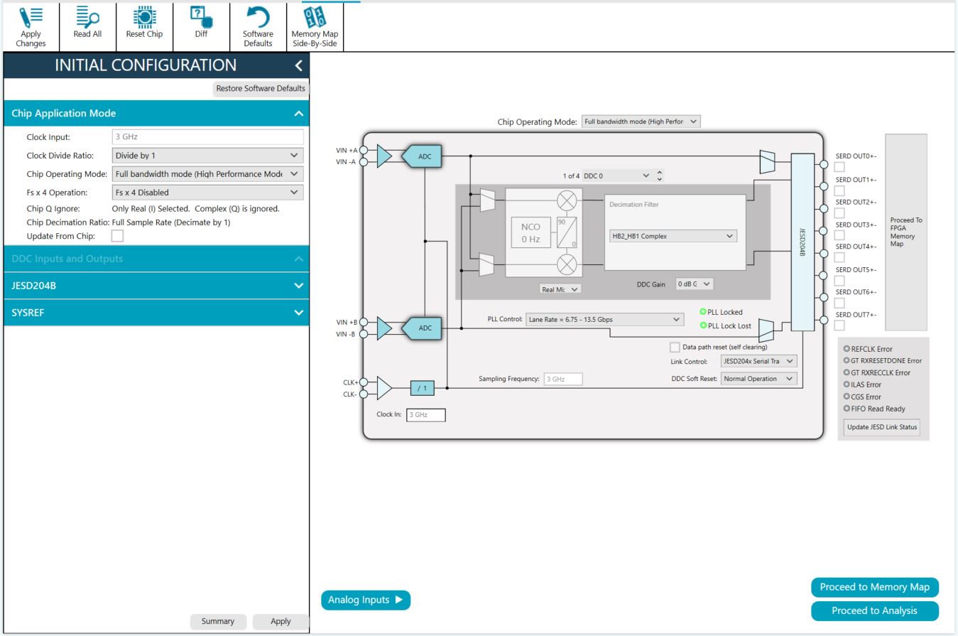
Figure 10 AD9208 Chip View (the AD9689 Chip view is similar)
Obtaining a full bandwidth capture
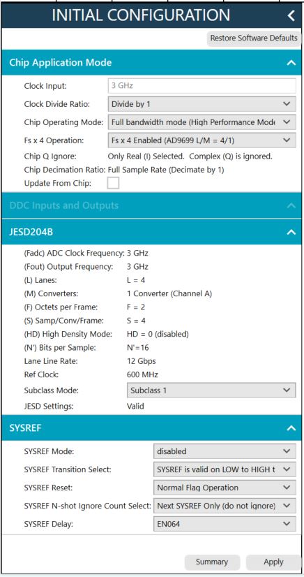
Under Initial Configuration, change the number of Virtual Converters to 1. Click Apply to apply the chip settings. Set the reference clock to the appropriate frequency as recommended by the ACE plugin.
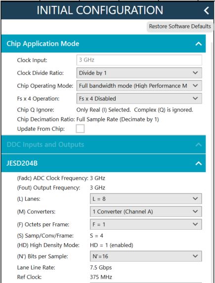
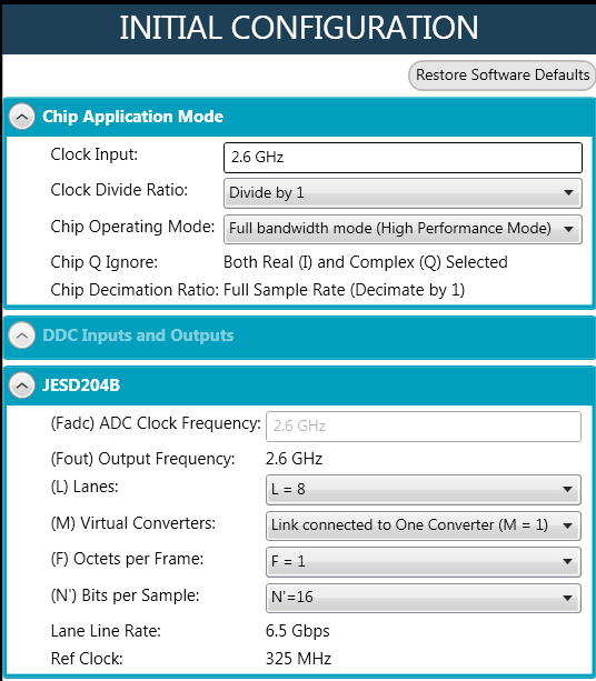
Figure 11 Chip Settings, AD9208-3000 on top, AD9689-2600 on bottom
The chip view will update to reflect the changes made to the board. If any changes are made, the chip can be read by clicking the Read All button.

Issue a data path reset to the AD9208 by clicking its checkbox and clicking Apply Changes. The data path reset bit will automatically self clear.
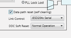

If the PLL Lock Lost indicator lights up, you can reset it by powering down the JESD link using the Link Control dropdown box, and clicking Apply Changes.
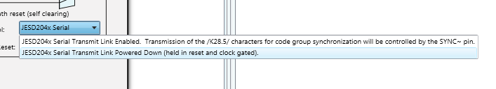
Enable the link again and Apply Changes.
Click Proceed to Analysis. This is ACE’s Analysis tool for data from the ADC, displaying both sample plots and FFTs. Click on FFT and run one capture.


Important
Capturing data using another program (e.g. VisualAnalog, proprietary code, etc.) while using ACE concurrently may cause errors in ACE’s data capture. If this occurs, the best solution is to restart the evaluation boards and work solely via ACE, or to setup the part in ACE then capture solely in the other program.
A successful capture is shown below, with a filtered 255 MHz signal input to Channel A.
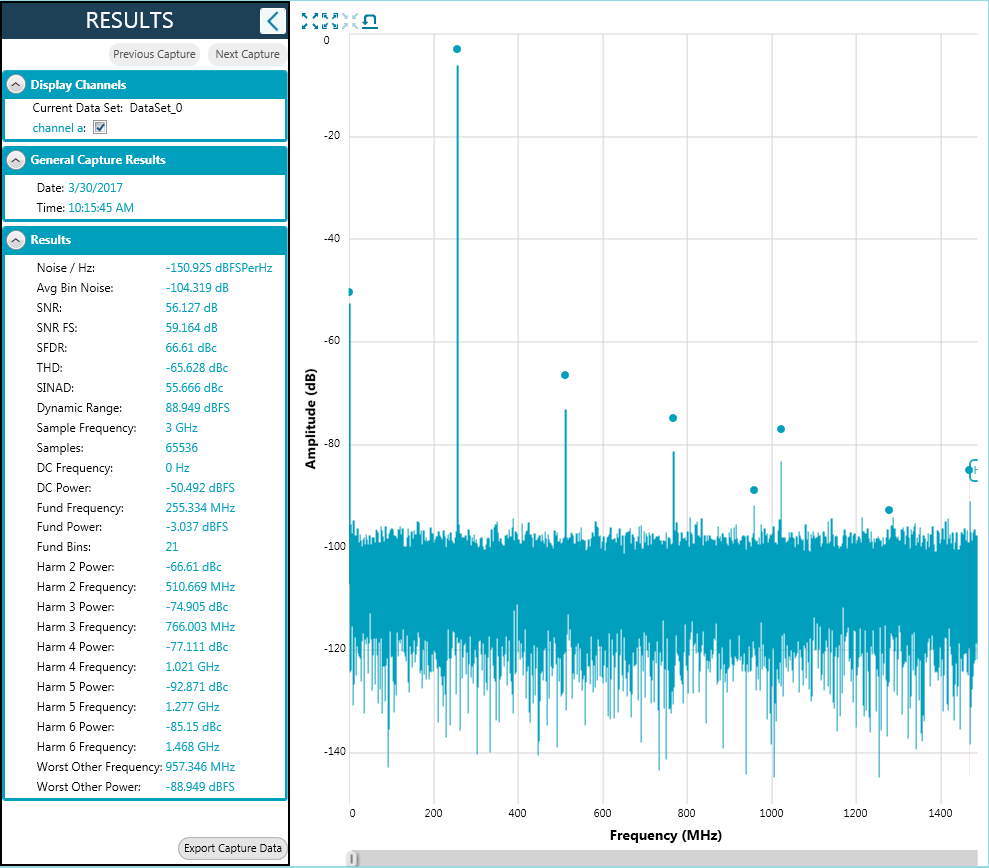
Figure 22 AD9208-3000 FFT at 255 MHz Analog Input to Channel A
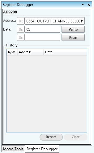
In order to get a capture from Channel B, use the Register Debugger within ACE and write 0x01 to register 0x0564. Click the Read All button. Repeat Step 6.
Obtaining a DDC capture
The procedure to obtain a FFT using DDC is the same between AD9208 and AD9689. The steps below use the AD9208 as the example, but the same can be done to the AD9689 plugin with the sample rate set to 2.6 GSPS.
This section explains the steps needed to setup the AD9208-3000EBZ in a DDC (Digital Down Converter) setup as shown in Figure 24.
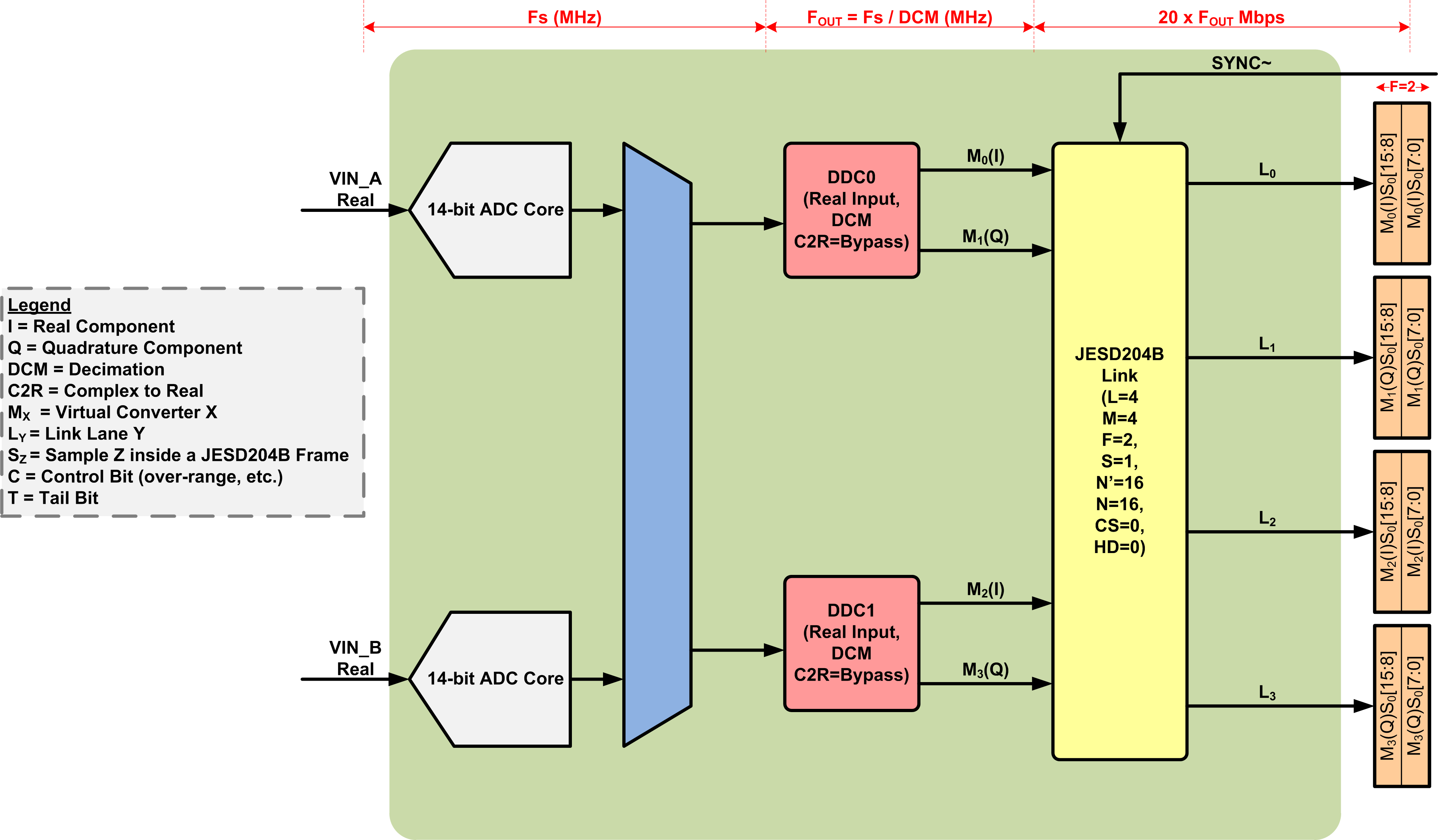
Under Initial Configuration, set the Chip Operating Mode for two DDCs. For AD9699, set the DDC inputs to Channel A only. The DDC settings will become available, and automatically set up for Decimate-by-4 mode. For the decimation, select “HB1_HB2_HB3 Complex” - three half-band filters, i.e. Decimate-by-8. Set the number of lanes to 4, the number of converters to 4, and the number of Octets per Frame to 2. Apply the settings.
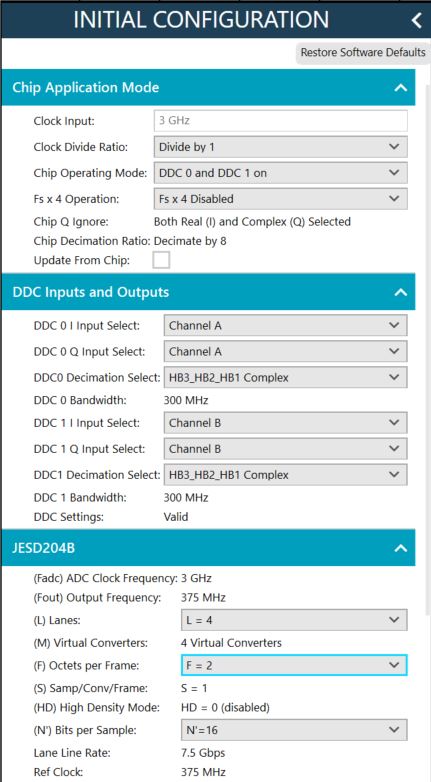
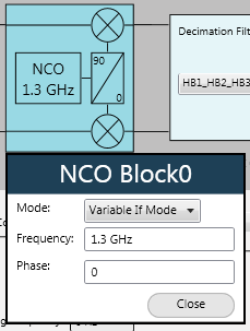
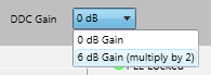
The chip view will update to reflect the changes. Click on the NCO block to change the Numerically Controlled Oscillator’s frequency to 1300 MHz. Enable the 6 dB gain for the DDC from the dropdown menu. Click Apply Changes to apply both.
Navigate to the second DDC (DDC1) and make the same changes.
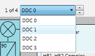
In Analysis, run a capture. DDC0 can be selected from Channel A and DDC1 can be selected from Channel B.
A successful capture is shown below, with a filtered 1305 MHz signal input to Channel A / DDC0.
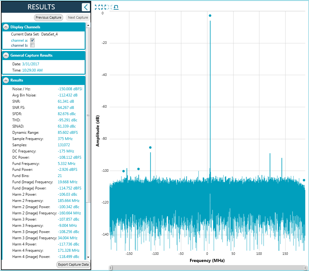
Figure 30 AD9208-3000 DDC FFT at 1305 MHz Analog Input to Channel A; NCO tuning frequency = 1300 MHz
Setting up AD9208/AD9699 Fsx4 mode
Fsx4 mode on AD9208/AD9699 is only supported using ADS8-V1EBZ. The procedure below shows how to use Fsx4 mode with ADC sampling frequency of 3 GHz and a Reference clock of 600 MHz.
On the Chip Application Mode tab, click on the Fsx4 Operation dropdown menu and select “L/M = 4/1” for AD9699, “L/M = 8/2” for AD9208.
Source the required REFCLK to the ADS8-V1EBZ.
Click Proceed to Analysis. This is ACE’s Analysis tool for data from the ADC, displaying both sample plots and FFTs. Click on FFT and run one capture.
A successful capture is shown below, with a filtered 255 MHz signal input to Channel A.
Figure 32 AD9208-3000 Fsx4 FFT at 255 MHz Analog Input to Channel A
Troubleshooting
Evaluation board isn’t functioning properly
It is possible that a board component has been rendered inoperable by ESD, removing a jumper during powered operation, accidental shorting while probing, etc. Try checking the supply domain voltages of the board while it is powered. They should be as follows:
Domain |
Jumper |
Test Point |
Approx. Voltage |
|---|---|---|---|
AVDD_1 |
P307 |
TP303 |
0.975 V |
AVDD_2 |
P308 |
TP304 |
1.90 V |
AVDD_3 |
P309 |
TP305 |
2.50 V |
DRVDD_1 |
P304 |
TP301 |
0.975 V |
DRVDD_2 |
P311 |
TP306 |
1.90 V |
DVDD |
P305 |
TP302 |
0.975 V |
SPI_VDD |
P312 |
TP307 |
1.90 V |
If a short is detected between any of the supply domains and ground, or an open is detected across fuse chip F401 (next to P401), a component may have been damaged. This may have occurred from jumper or board removal while being actively powered. See the Design and Integration Files section for the schematic and/or bill of materials for the relevant components to test and/or replace.
Evaluation board is not communicating with the ADS7-V2EBZ
Make sure that the FPGA on the ADS7-V2EBZ has been programmed - a lit LED DS15 (FPGA_DONE) on the top of the ADS7-V2EBZ and a powered fan are good indicators of the FPGA being programmed.
Check the common mode voltage on the JESD204B traces. On the evaluation board, the common mode voltage should be roughly two-thirds of DRVDD_1. On the ADS7-V2EBZ, the common mode voltage should be around 1.2 volts.
Check Test Point 307 - test point for the SPI_VDD supply domain, jumper P312 - and make sure it is around 1.9 volts.
To test SPI operation, attempt to both read and write to register 0x000A using ACE’s Register Debugger (see Figure 23). This register is an open register available for testing memory reads and writes. If the register reads back the same value written to it, SPI is operational.
All registers reading back as either all ones or all zeros (i.e., 0xFF or 0x00) may indicate no SPI communication.
Register 0x0000 (SPI Configuration A) reading back 0x81 in ACE may indicate no SPI communication as a result of the FPGA on the ADS7-V2EBZ not being programmed.
Evaluation board fails to capture data
Ensure that the board is functioning properly and that SPI communication is successful - see previous troubleshooting tips.
Check the Clock Detect register 0x011B to see if the sample clock is being detected. 0x01 indicates detection, 0x00 indicates no clock detected. Check the signal generator input on connector J201. Try checking the common mode voltage on the clock pins, which should be roughly two-thirds of AVDD_1. Try placing a differential oscilloscope probe on the clock pins to see if the clock signal is reaching the chip.
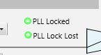
Check the PLL Locked indicator (see Figure 16) or register 0x056F (PLL Status). If the light in the plugin chip view is green / if the register reads back 0x80, the PLL is locked. If it is not locked:
Check the clock being input to connector J201 (in this guide, 3 GHz or 2.6 GHz depending on the part).
Check the JESD204B settings under the Initial Configuration. Reference the AD9208 / AD9689 / AD9699 datasheet for supported lane options.
Check the reference clock and make sure it matches your JESD settings.
Make sure P100 (Power Down / Standby Jumper, see Figure 6) is not jumped.