ADAR1000 Beamforming Board
The ADAR1000EVAL1Z (Stingray) is the analog beamforming heart of the X-Band platform, providing 32-channel transmit and receive capability with individual phase and amplitude control.
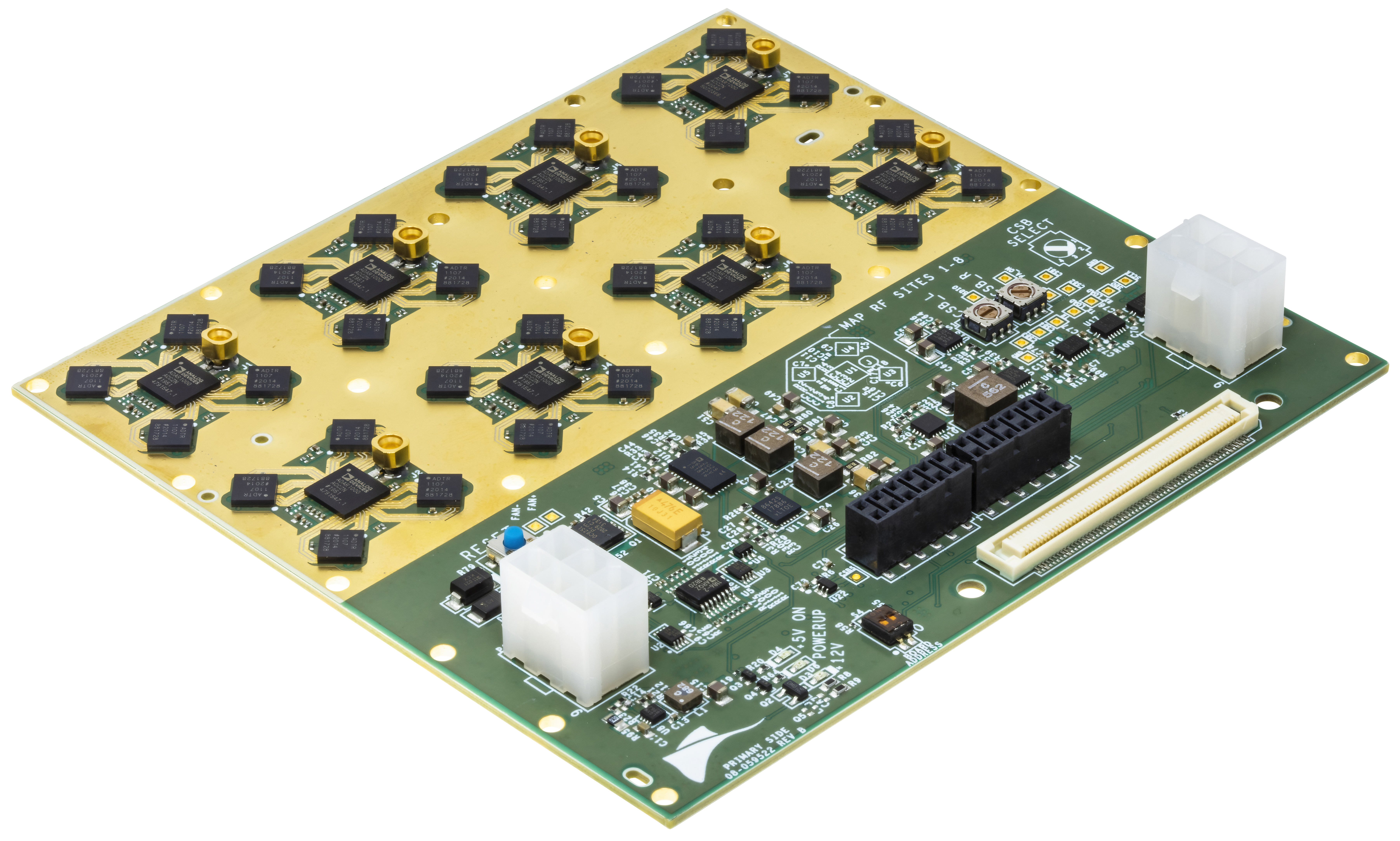
Overview
The ADAR1000EVAL1Z, nicknamed “Stingray,” is a comprehensive analog beamforming evaluation platform built around eight ADAR1000 beamforming ICs. Each ADAR1000 is surrounded by four ADTR1107 front-end modules (PA + LNA + TR switch), providing 32 independent TX/RX channels operating across 8–16 GHz (X/Ku-Band).
Tip
Schematics & Reference Documents
:git-linux:
Linux IIO Driver (source) <drivers/iio/beamformer/adar1000.c>
Component Product Pages
ADAR1000 - 8 GHz to 16 GHz, 4-Channel, X/Ku Band Beamformer
ADTR1107 - 6 GHz to 18 GHz Front-End IC (PA + LNA + TR Switch)
HMC948 - GaAs Log Detector
ADA4807-1 - Unity Gain Buffer Op-Amp
LTC2314-14 - 14-Bit, 4.5 Msps Serial ADC
LT8652S - Dual-Channel Synchronous Step-Down Converter
LT8642S - 18V, 10A Synchronous Step-Down Regulator
LT3093 - Negative Linear Regulator
LT3094 - Negative Linear Regulator
LT8606 - 42V, 350mA Step-Down Regulator
ADP150 - Ultralow-Noise Linear Regulator
ADP5074 - Inverting Regulator
ADM1172 - Hot-Swap Controller
ADM1186 - Quad Voltage Sequencer
LTC2992 - Power Monitor with GPIO
LTC4301 - I2C Hot-Swappable Bus Buffer
ADAR1000 IC Quick Reference
Parameter |
Value |
|---|---|
Frequency Range |
8 GHz – 16 GHz (X / Ku Band) |
Channels |
4 per IC (8 ICs → 32 channels on Stingray) |
Duplex |
Half-duplex (TX ↔ RX, single-pin control) |
Phase Control |
360° range, 2.8° resolution |
Gain Control |
≥ 31 dB range, ≤ 0.5 dB resolution |
Beam Memory |
121 pre-stored beam positions |
Power Detectors |
4× (−20 dBm to +10 dBm) with integrated 8-bit ADC |
Interface |
4-wire SPI (up to 4 devices per bus via address pins) |
Package |
88-terminal LGA, 7 mm × 7 mm |
Operating Temp |
−40 °C to +85 °C |
Key Features
Array Architecture
32 Channel Analog Phased Array Prototyping Platform
8× ADAR1000 Analog Phased Array Beamforming ICs
32× ADTR1107 Transmit/Receive ICs (6–18 GHz front-end module)
RF In, RF Out Design
Individual RFIO for each BFIC
Physical Design
2× ADAR1000EVAL1Z-ANT with 10 GHz lattice spacing antenna tiles
32× SMPM Bullets for direct antenna connection
Heatsink and H-Frame mechanical hardware included
Control and Calibration
Stand-Alone RF Detector/ADC Combo (HMC948 + ADA4807-1) for calibration
PMOD Connectors (P3, P4) for programming
SDP-S Connector (P5) for standalone evaluation
Individual channel control for phase and amplitude
Board Layout
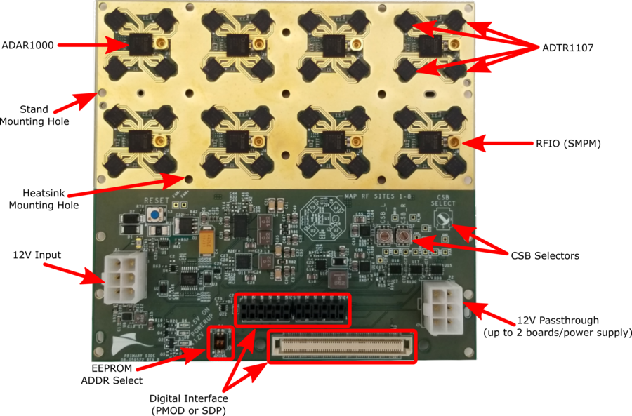
Figure 2 Component Side Overview — ADAR1000 ICs, ADTR1107 front-ends, power regulation, and control connectors
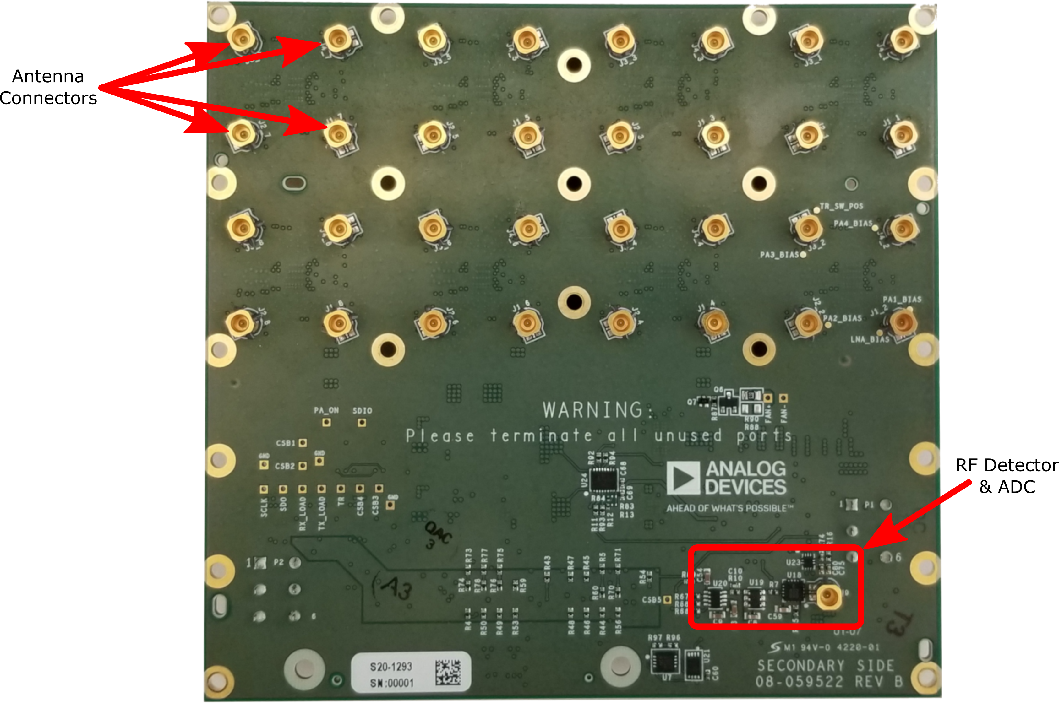
Figure 3 Antenna Side Overview — 32 SMPM antenna connectors and RF shielding
Physical Interface
Connectors
Connector |
Type |
Function |
|---|---|---|
J1–J8 |
SMPM |
ADAR1000 RFIO (one per IC) |
32× Antenna |
SMPM |
Individual element antenna ports |
J9 |
SMPM |
RF detector input |
P1, P2 |
6-pin Molex |
12V DC power (dual for daisy-chain) |
P3, P4 |
PMOD |
Digital control (3.3V logic) |
P5 |
SDP-S |
Alternative digital control |
PMOD Pinout

Figure 4 PMOD Connector Pinout — 3.3V logic with on-board level translation to 1.8V for ADAR1000 SPI
SPI Architecture
Five chip-select lines control the board:
CSB Line |
Function |
|---|---|
CSB1–CSB4 |
ADAR1000 IC control |
CSB5 |
RF detector / ADC |
Two selector switches (S1, S2) route CS lines to left and right cell groups, enabling control of all 8 ADAR1000 ICs using a minimum of two CSB lines.
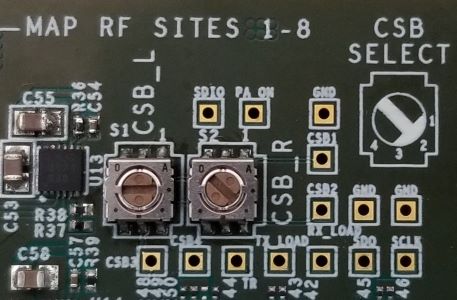
Figure 5 CSB Selector Switches (S1, S2) — Route chip-select to left/right cell groups
Array Configuration
Subarray Layout
The Stingray board provides a 4×8 array configuration with two ADAR1000s per subarray:
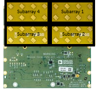
The four subarrays (1–4), each driven by a pair of ADAR1000 ICs. Every subarray can be independently configured as RX, TX, or OFF. |
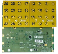
Individual element mapping across the 32-channel array, showing physical antenna element positions and their corresponding channel assignments. |
Channel Mapping
Understanding the relationship between ADAR1000 IC channels and system-wide Stingray channel numbers is critical for programming and debugging:
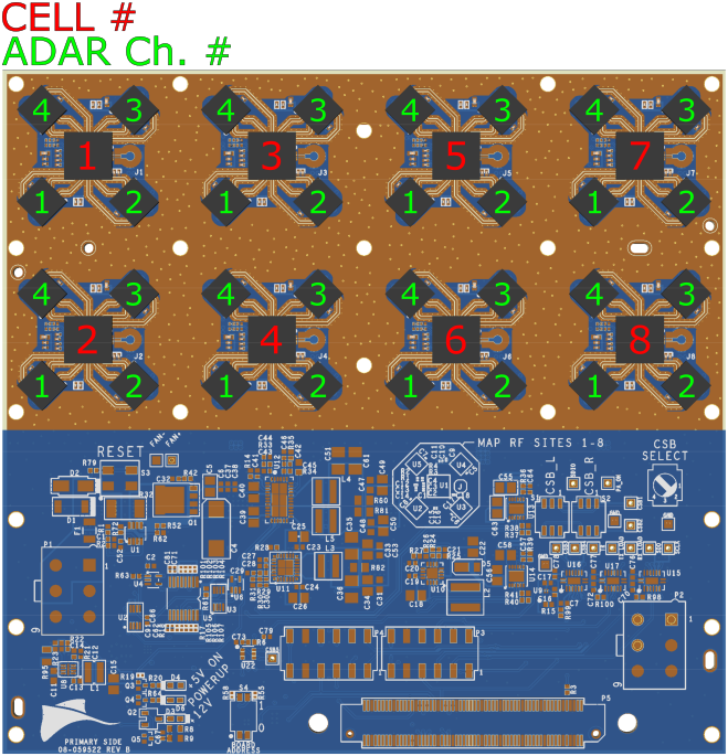
Cell Map — In the Linux device tree, each ADAR1000 IC (cells 1–8, green) exposes 4 sub-attributes that control its individual ADTR1107 front-ends. The red numbers (1–4) show how those sub-attributes are referenced per IC. |
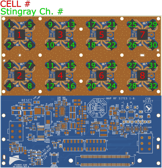
Channel Map — The same physical layout with system-wide Stingray channel numbers (1–32, green) overlaid on their parent cell numbers (red). Use these channel numbers when configuring beamforming in software. |
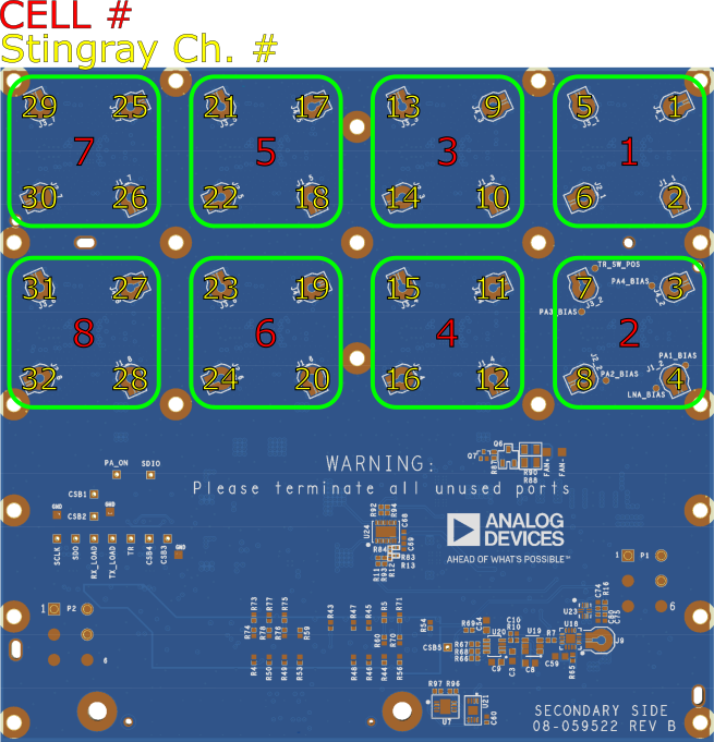
Figure 6 Reverse Channel Mapping — Antenna-side view showing element-to-channel correspondence
Power Sequencing
Warning
PA damage risk. The ADAR1000s MUST be initialized to put the ADTR1107 PAs in a safe (pinched-off) state BEFORE the +5V rail is enabled. Failure to follow this sequence can damage the ADTR1107 power amplifiers.
Power-Up Sequence
Step |
Action |
Result |
|---|---|---|
1 |
Apply 12V to P1 |
Enables 3.3V, 1.8V, −6V rails |
2 |
Configure LTC2992 GPIO to Hi-Z |
Prevents premature rail enable |
3 |
Pulse PWR_UP_DOWN |
Enables 3.3V, −3.3V, −5V rails |
4 |
Initialize all ADAR1000s via SPI |
PAs pinched off, safe state |
5 |
Pulse +5V_CTRL |
Enables +5V PA supply rail |
Important
LTC2992 GPIO must be Hi-Z before any power sequencing begins. Failure to configure this causes an indeterminate board state requiring hard reset.
Automatic Sequencing
The ZCU102 firmware includes an embedded power sequencing script that handles steps 2–5 automatically on boot. The script:
Configures LTC2992 GPIO to Hi-Z
Pulses PWR_UP_DOWN with proper timing
Initializes ADAR1000 registers via SPI
Enables +5V_CTRL only after safe initialization
Manual Power Control
Power Down: Press RESET button on primary side of board
Power Up: Controlled via firmware script on ZCU102 boot
Support ICs
Component |
Function |
|---|---|
LTC2992 |
Power monitor — GPIO controls rail sequencing |
ADM1172 |
Hot-swap controller |
ADM1186 |
Sequencer / voltage supervisor |
LTC4301 |
Hot-swappable I2C buffer |
LT8652S |
Dual-output step-down regulator |
LT8642S |
Step-down regulator |
LT3093/LT3094 |
Negative LDO regulators |
LT8606 |
Step-down regulator |
ADP150 |
Low-noise LDO |
ADP5074 |
Dual-output regulator |
ADAR1000 Initialization
Each ADAR1000 requires SPI configuration at power-up to establish a safe operating state:
Reset and LDO adjustment — Soft reset, configure internal LDO voltage
Bias point setup — Set PA bias (pinched off initially) and LNA bias
Channel gain and phase configuration — Default gain/phase per channel
TR control mode selection — Set TX/RX switching mode (SPI or pin-controlled)
RF Performance
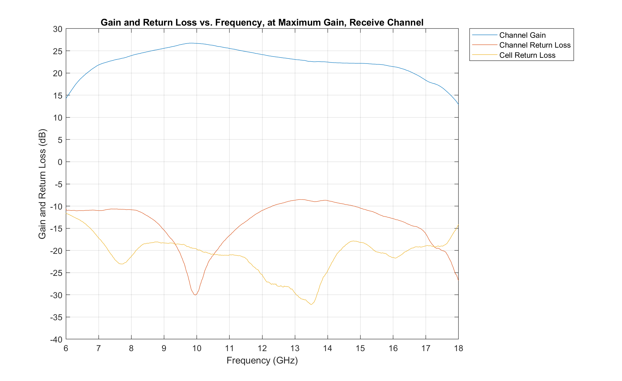
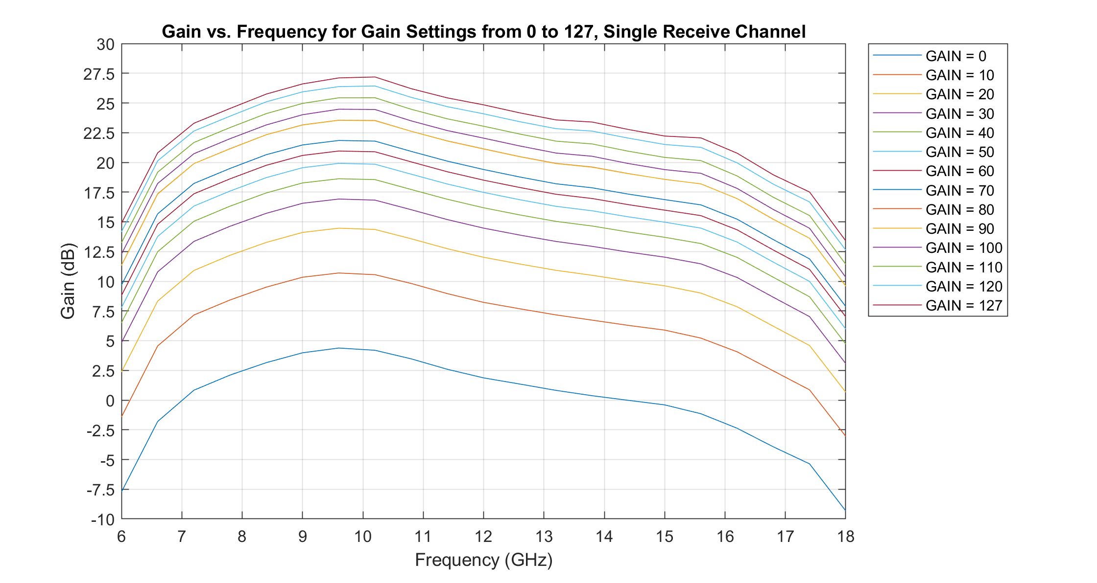
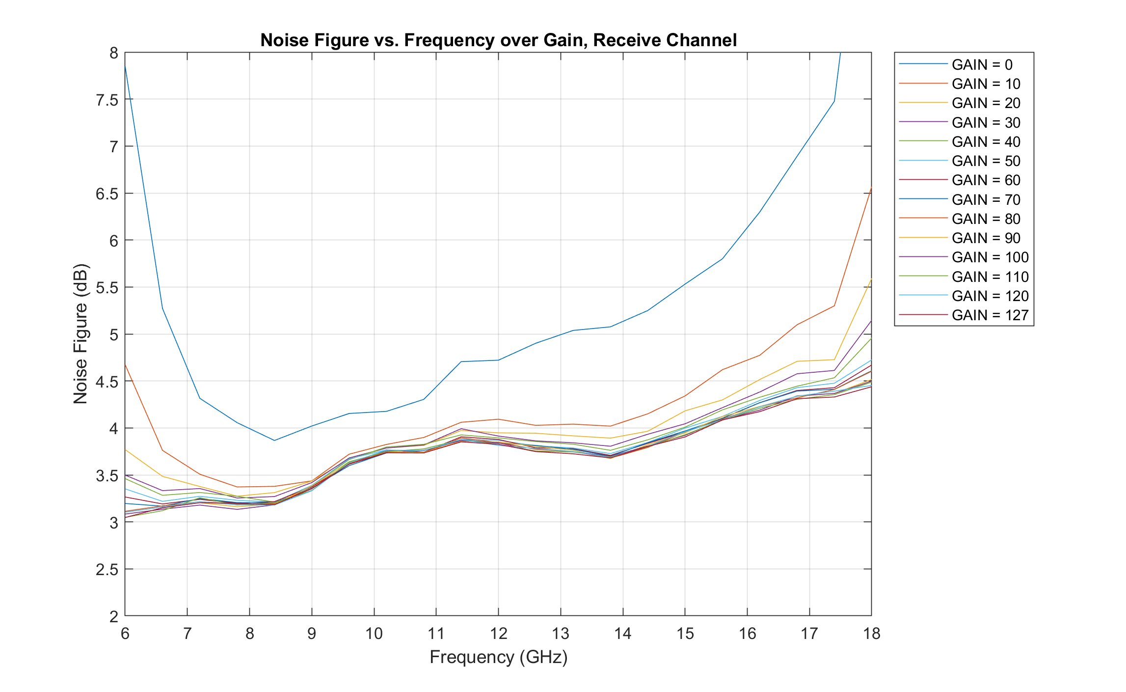
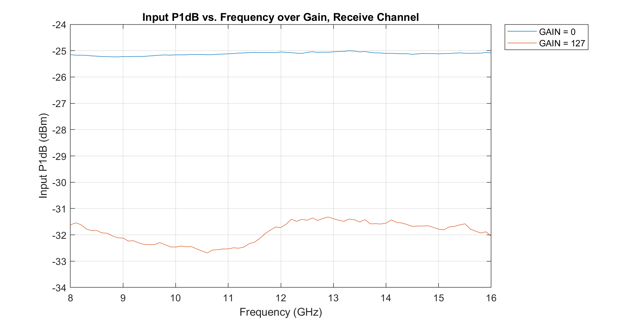
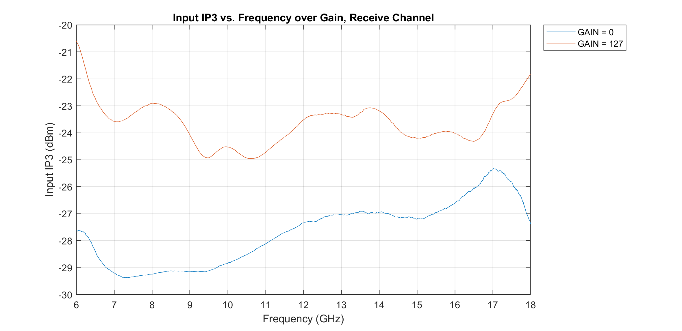
Receive Mode
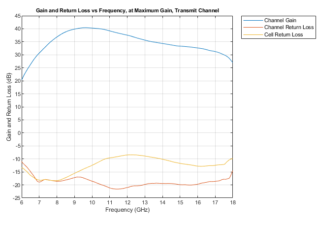
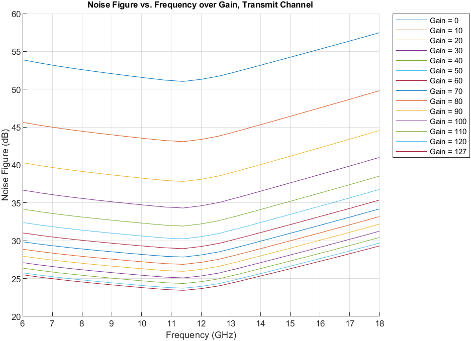
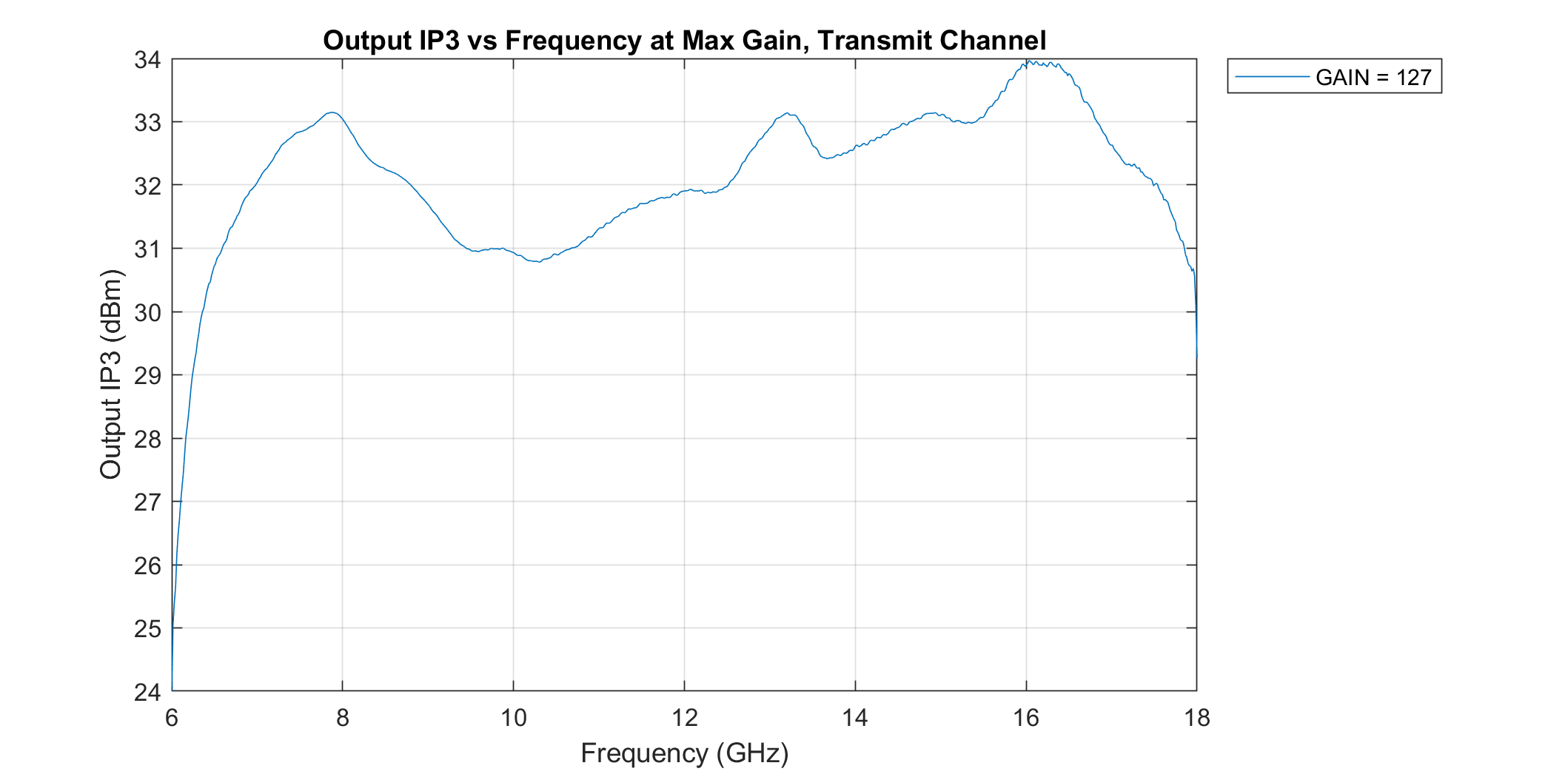
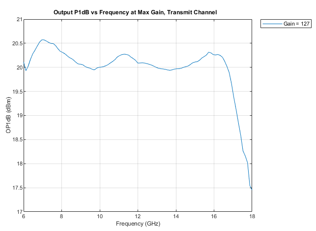
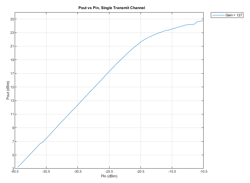
Transmit Mode
Switching Speed
TX/RX switching measurements at 10 GHz with 4 coherently combined channels (1 kHz PRI, 50 µs pulse width):
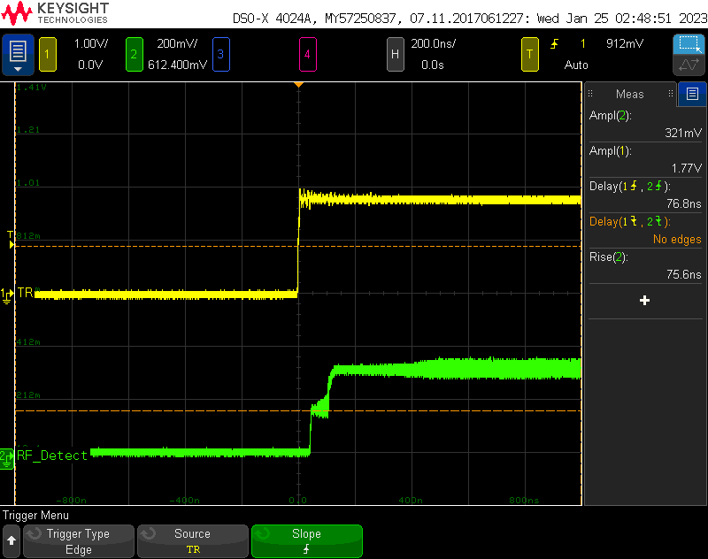
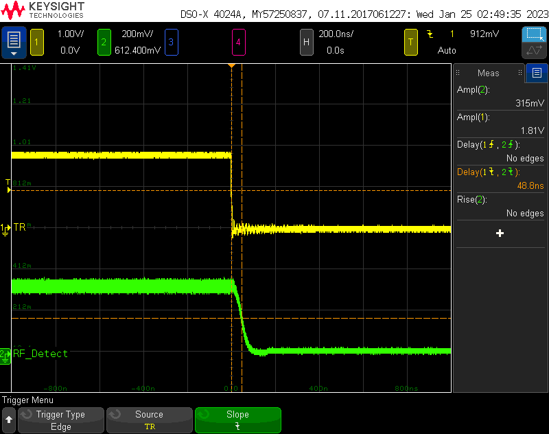
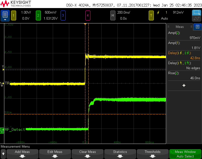
Figure 19 RX→TX Switching (200 ns/div) — 4 channels, −7 dBm input
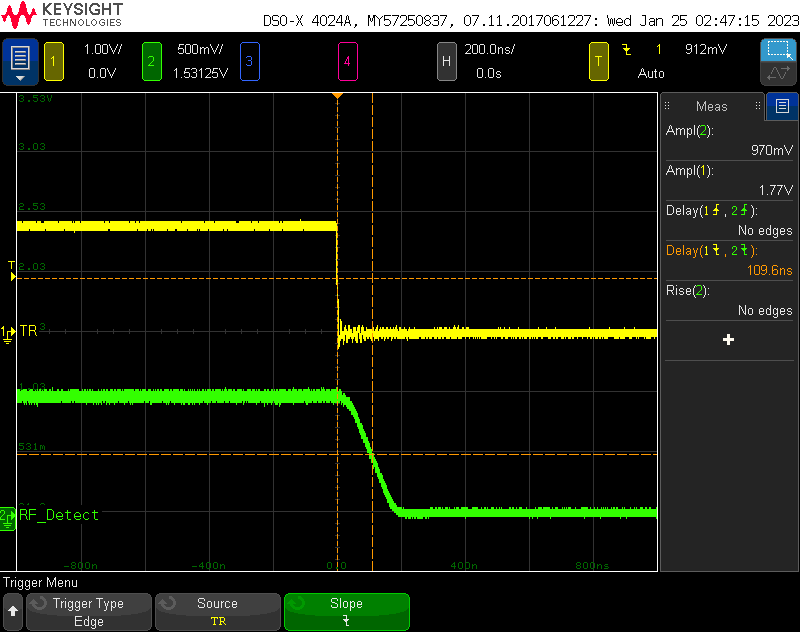
Figure 20 TX→RX Switching (200 ns/div) — 4 channels, −7 dBm input
TDD Operation
The Stingray board operates in Time Division Duplex (TDD) mode, switching between transmit and receive states based on control signals from the ZCU102.
TR Probe Point
For TDD measurement and debugging:
Location: Secondary side of ADAR1000EVAL1Z board
Signal: TR_EN probe point
Purpose: Monitor transmit/receive switching timing
Thermal Management
Important
The Stingray board generates significant heat during operation:
Heatsink installation is required for proper operation
Cooling fans (3× 120mm) are recommended for extended operation
Thermal shutdown protection is built into the ADAR1000 ICs