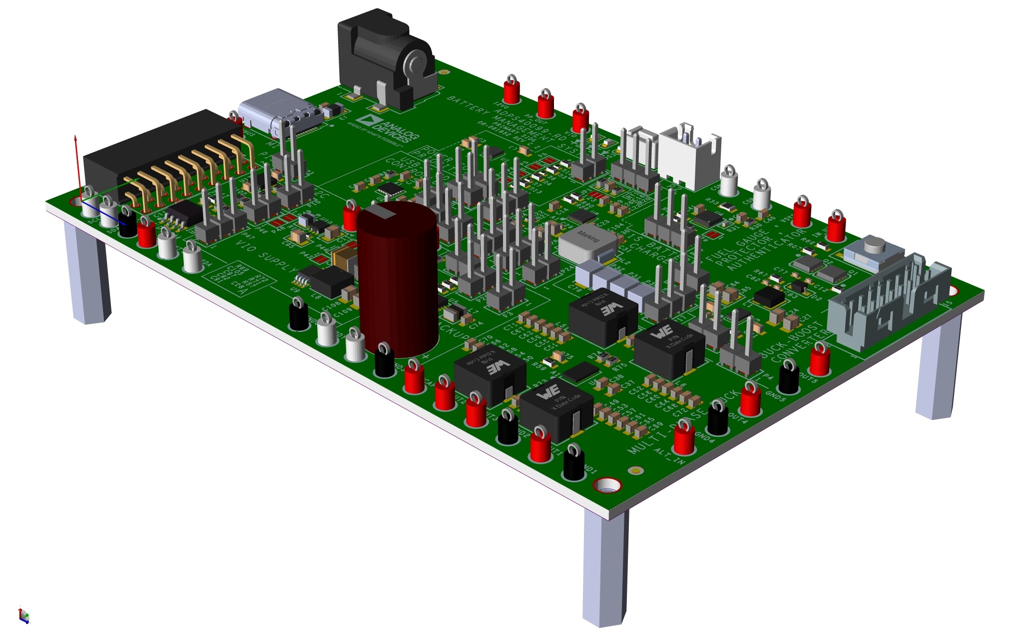
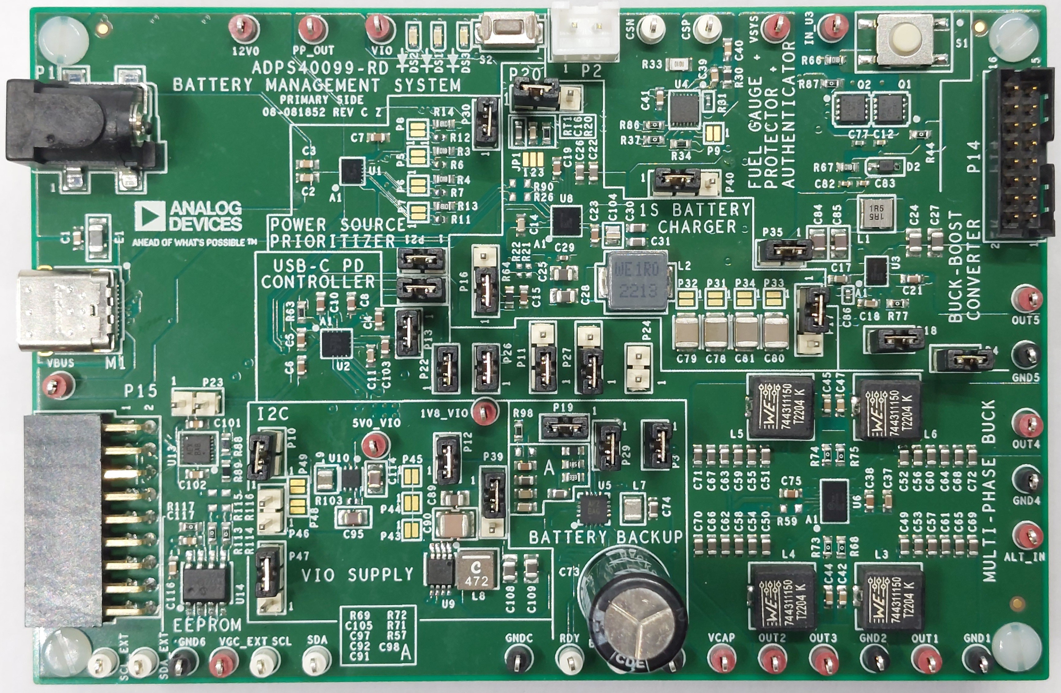
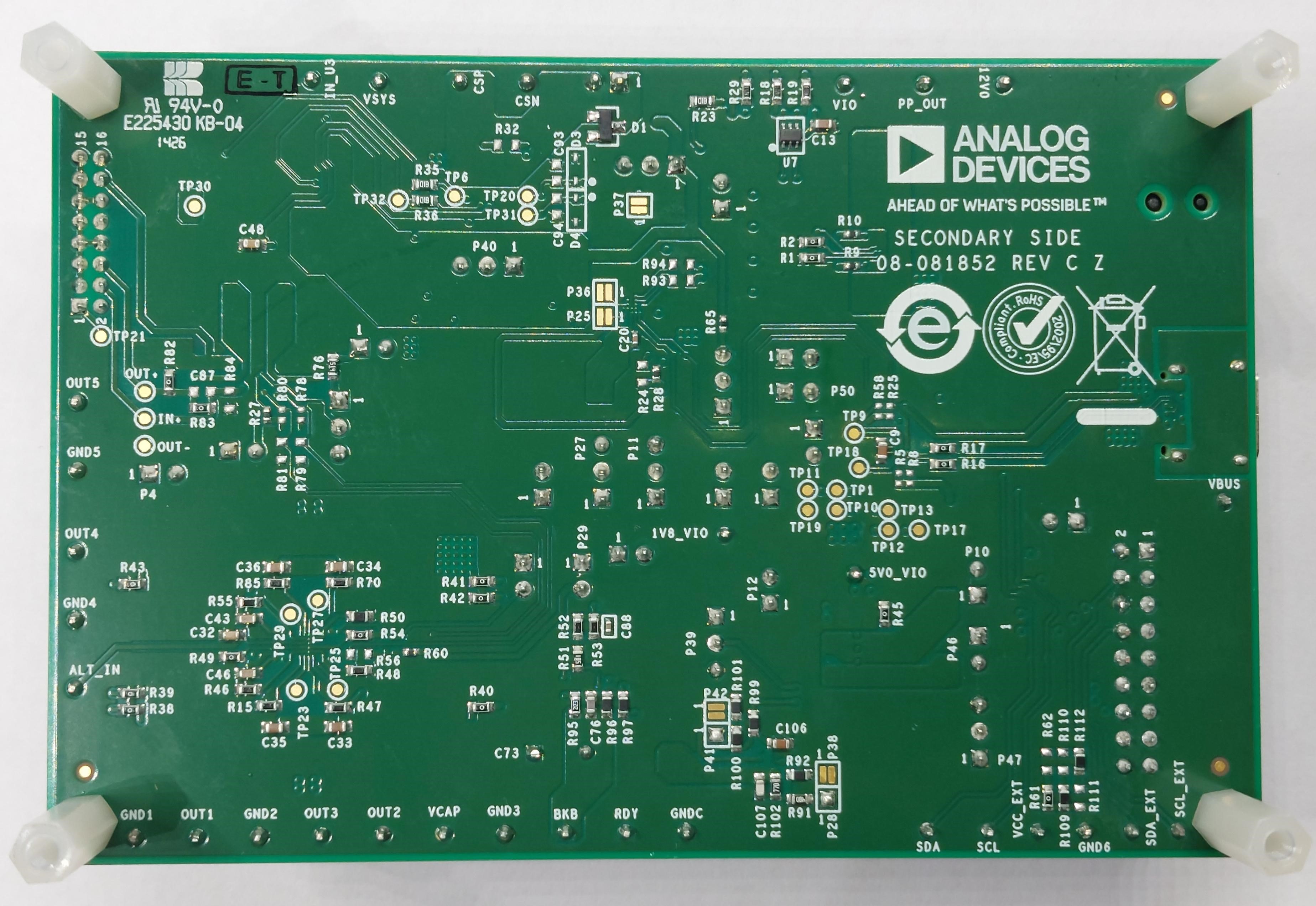
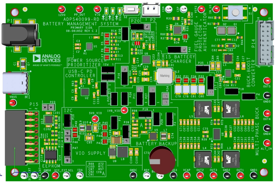
The ADPS40099-RD is a fully integrated battery management
system reference design for portable applications. It combines a complete
power solution for handheld and portable devices, using the latest components
from ADI’s power portfolio.
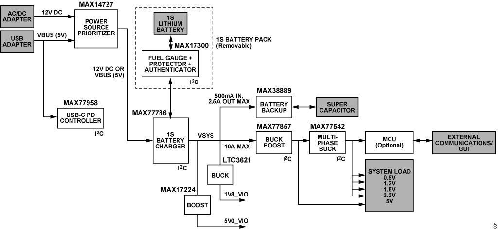
The solution features the MAX77958 USB-C power delivery controller for flexible
input options, paired with the MAX77786 1S battery charger to manage charging
from a single-cell lithium-ion battery. The MAX17300 provides advanced fuel
gauging, battery protection, and authentication capabilities, ensuring safe and
reliable operation.
To support diverse power requirements, the design includes the MAX77857
buck-boost regulator and the MAX77542 multi-phase buck converter, enabling up to
five individually configurable outputs. The design also integrates the MAX14727
for power path control. For backup power, the MAX38889 uses supercapacitor
technology to maintain system operation during power interruptions and battery
replacements. Additionally, the MAX14611 logic-level translator ensures seamless
communication between components operating at different voltage levels.
This compact, cohesive single-board implementation delivers a robust,
space-efficient, and scalable battery management solution ideal for modern
portable electronic systems.
System Features
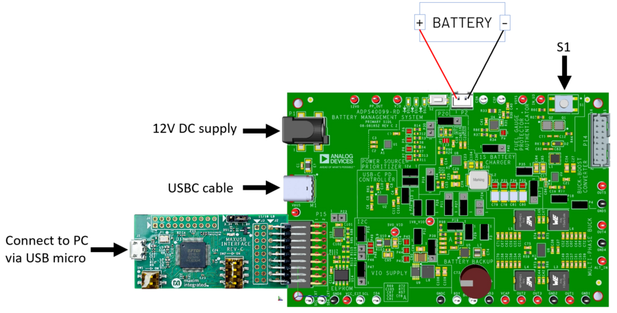
Power Supply Options: Supports both USB-C with Power Delivery and 12V DC input
Input Priority: USB-C takes precedence over DC input
Battery Type: Single-cell (1S) Lithium-Ion
Charging Current: Up to 5A, user-configurable via I²C
Connects buck
input directly to
MAXUSB interface
supply
P45
Alternative Buck
Input
open
Connects buck
input to power
prioritizer
output
P48
Alternative Boost
Input
open
Connects boost
input directly to
battery positive
P44
Alternative Boost
Input
open
Connects boost
input directly to
MAXUSB interface
supply
Featured ADI Devices
Power Prioritization and Protection
The MAX14727 functions as both a power
prioritizer and protector on the board. It automatically selects USB-C (Channel
A) as the preferred input over 12V DC (Channel B), while protecting the system
from overvoltage conditions (up to +28V) and surge events (up to 100V). It also
prevents reverse current, supports OTG functionality, and includes adjustable
overvoltage thresholds and thermal shutdown for enhanced system reliability.
USB-C PD Controller
The MAX77958 serves as the USB-C Power Delivery (PD) controller on the board.
It handles USB-C CC detection, PD negotiation, overvoltage/overcurrent protection,
and moisture detection. It also supports legacy USB standards, OTG, and
alternate mode configuration. With built-in I²C master capability,
it can autonomously configure related devices without host intervention.
1S Battery Charger
The MAX77786 is the board’s main battery
charger, supporting fast charging up to 5.5A with Smart Power Selector™. It
enables efficient charging, reverse-boost operation, and supports various
battery chemistries. The charger is highly configurable via I²C and includes
features such as BC1.2 detection, load disconnection, and dead-battery startup.
Battery Backup
The MAX38889 manages supercapacitor-based
backup power for the board. It charges the storage element when input power is
available and seamlessly boosts its voltage to maintain system operation during
power loss or battery swaps. It supports up to 3A peak current and is
configurable for a variety of backup voltage and current settings.
Fuel Gauge & Battery Authentication
The MAX17300 is a low-power, pack-side fuel
gauge and SHA-256 battery authenticator for 1-cell Li-ion/polymer batteries. It
uses the ModelGauge m5 algorithm, combining coulomb counting and voltage-based
measurements for highly accurate state-of-charge (SOC) reporting. The device
also supports dynamic power reporting, providing real-time estimates of the
maximum power the battery can safely deliver. Communication and configuration
are handled via an I²C interface for secure and intelligent battery management.
5V Output Regulator
The MAX77857 is a high-efficiency buck-boost
converter used to provide a regulated 5V output on the board. It supports a wide
input voltage range of 2.5V to 16V, delivering up to 6A in buck mode and 4A in
boost mode, with optional I²C control for dynamic voltage adjustment.
Multi-Rail Power Supply
The MAX77542 is a high-efficiency step-down
converter used to generate key output rails (3.3V, 1.8V, 1.2V, and 0.9V)on the
board. It supports a wide input voltage range from 2.8V to 16V, making it
suitable for USB PD and Li-ion battery sources. Output voltages are preset via
resistors and adjustable through I²C from 0.3V to 5V.