User Guide for the AD7944/AD7985/AD7986
14-/16-/18-Bit PulSAR ADCs
Features
PC control with EVAL-CED1Z converter board
Software for time and frequency domain analysis
Versatile analog signal conditioning circuitry
On-board reference, clock oscillator, and buffers
Standalone capability
System Requirements:
Windows XP SP2, Vista, or Windows 7
USB 2.0 port
Software Needed:
Enclosed CD or website download
Evaluation Kit Contents:
Evaluation board (EVAL-AD7944EDZ, EVAL-AD7985EDZ, or EVAL-AD7986EDZ)
Software CD
Documents Required:
Equipment Required:
Precision DC and AC signal sources
Band-pass filter (16-/18-bit rated)
SMB cable
EVAL-CED1Z board
7V DC supply adapter
General Description
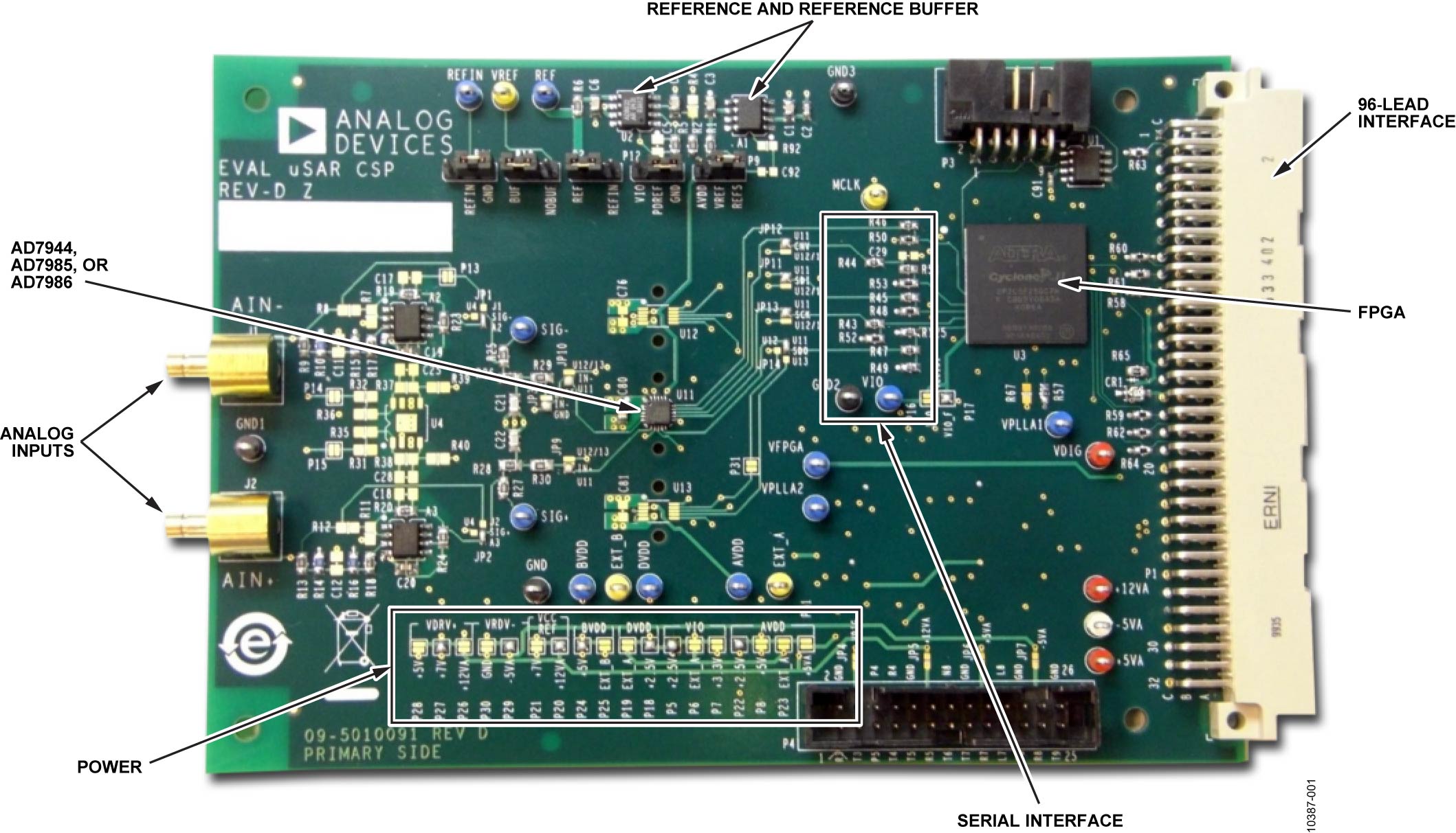
The EVAL-AD79XXEDZ evaluation board targets 20-lead PulSAR ADCs. On-board components include a high precision, buffered band gap 5.0V reference (ADR435), reference buffers (AD8032), a signal conditioning circuit with two op-amps (AD8021), and an FPGA for deserializing the serial conversion results. This evaluation board interfaces to the EVAL-CED1Z capture board via a 96-pin DIN connector. SMB connectors are provided for the low-noise analog signal source.
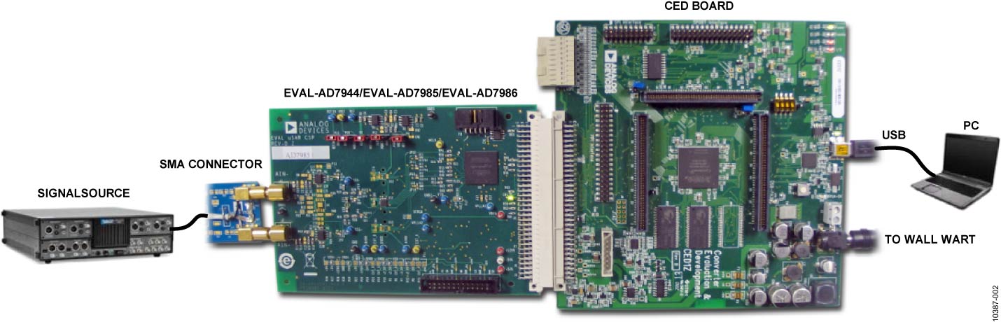
Figure 2 EVAL-AD7944/AD7985/AD7986 evaluation board block diagram
The AD7944 is a 14-bit, 2.5 MSPS SAR ADC, the AD7985 is a 16-bit, 2.5 MSPS SAR ADC, and the AD7986 is an 18-bit, 2.0 MSPS SAR ADC. Each device features an internal conversion clock, an internal reference (and buffer), error correction circuits, and a versatile serial interface port.
Quickstart
Install the software from the CD or website download. Disconnect the evaluation board during installation.
Connect the EVAL-CED1Z to the evaluation board.
Connect the 7V power supply adapter to the EVAL-CED1Z connector J4.
Connect the EVAL-CED1Z via USB to the PC (drivers auto-detect).
Launch the evaluation software from the Programs menu.
Select the device from the dropdown (AD7944, AD7985, or AD7986).
Apply the signal source to the AIN+/AIN- SMB inputs.
Configure the signal source appropriately.
Initiate single capture (F3) or continuous capture (F4).
Configure the software per the Software Operation section.
Note
The measurements made by Analog Devices use the Audio Precision SYS-2522.
Evaluation Board Hardware
Power Supplies
Each supply is decoupled where it enters the board and again at each device. A single ground plane is used on this board to minimize the effect of high frequency noise interference.
Standalone Operation
The evaluation board can operate without the EVAL-CED1Z controller. It requires ±5V, +12V, +7V, or +2.5V power supplies (see the design support package for detailed connection information).
Grounding
The evaluation board ground plane is separated into two sections: a plane for the digital interface circuitry and an analog plane for the analog input and external reference circuitry. These planes are connected directly beneath the ADC converter to minimize noise coupling.
Conversion Control
The on-board FPGA performs a number of digital functions, one of them being the deserialization of the serial conversion results as the EVAL-CED1Z data capture board uses a 16-bit parallel interface.
Analog Inputs
The analog inputs J1 and J2 are SMB (push-on) connectors, buffered with dedicated amplifier circuitry (A2, A3) and discrete components as shown in the schematic. The circuit allows for different configurations:
Gain adjustment
Input range scaling
Filtering
Addition of a DC component
Use of different op-amps and supplies
The analog input amplifiers are set as unity-gain buffers at the factory, with supplies set for +7V to -5V ranges. Both A2 and A3 are set at midscale generated from a buffered reference voltage divider or internal ADC reference.
The AD7986 uses differential inputs; the AD7944 and AD7985 use a single-ended path.
For FFT testing, a very low distortion AC source is required. For low-frequency testing, an audio precision source can be used directly because the outputs on these are isolated.
Serial Interface
The 3-wire serial interface SDI, SCK, and SDO together with CNV are present on the digital interface test points, and FPGA-buffered versions are on the 96-pin connector, P1.
Jumpers, Solder Pads and Test Points
Reference Options
External Reference (Factory Configuration)
The board includes an ADR435 5V precision reference. The best attainable SNR is achieved by using the maximum reference voltage of 5V.
Jumper |
Setting |
|---|---|
P2 |
REF and middle |
P9 |
REFS to VREF |
P10 |
BUF to middle |
P11 |
REFIN to GND |
P12 |
PDREF to VIO |
BVDD |
5V (factory default) |
Two external reference methods are available:
Unbuffered: Leave P10-P12 as factory settings, open P2, connect source to REF test point.
Buffered: Replace P2, open P9, apply source to VREF test point.
ADC Reference Supply, BVDD
The board includes a 5V source at solder pads (5V or EXT_B) and test point EXT_B. For the best performance, derive this supply from the external reference.
Internal 4.096V Reference
The ADC has an internal 4.096V precision reference and can be used on most applications. Connecting PDREF to GND enables the internal reference.
Internal Reference Buffer
The internal reference buffer is useful when using an external 1.2V reference. Applying 1.2V to REFIN produces 4.096V at the ADC REF pin.
Method 1: REFIN Test Point
Jumper |
Setting |
|---|---|
P2 |
Open |
P9 |
Don’t care |
P10 |
Don’t care |
P11 |
Open |
P12 |
PDREF to VIO |
BVDD |
5V (factory default) |
Method 2: Divide Down
Uses U2 op-amp to divide 5V ADR435 output to 1.2V via R2/R4 = 1 kOhm/316 Ohm.
Evaluation Board Software
Pre-Installation
Important
The EVAL-CED1Z board must not be connected to the USB port of the PC until after the software is installed. The green LED on the board confirms power; connecting the 7V DC supply is acceptable before installation.
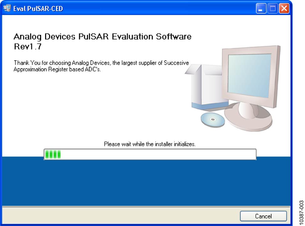
Software Installation
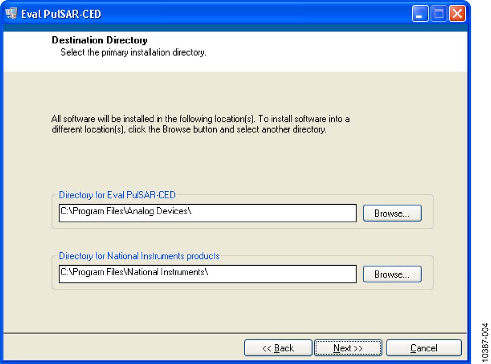
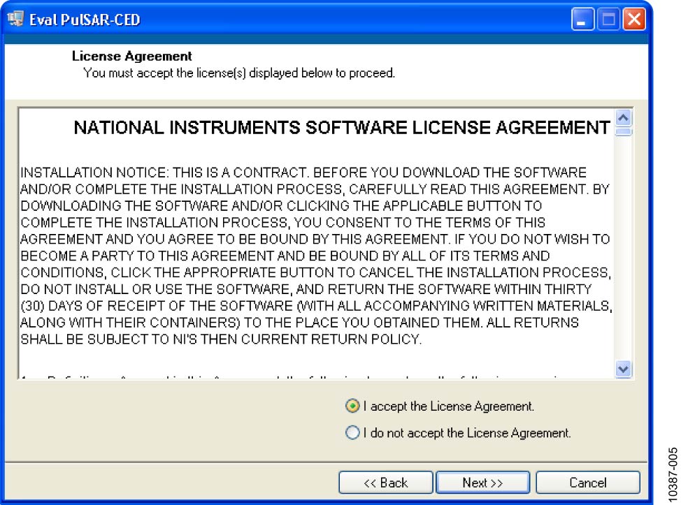
Close all Windows applications before installation. The CD is included; latest versions are also available on analog.com. The user must accept the license agreement during the installation process.
Extract the software using WinZip (rather than running setup.exe directly).
Run setup.exe from the extracted folder.
Follow the on-screen instructions.
Remove prior versions via Control Panel > Add or Remove Programs if needed.

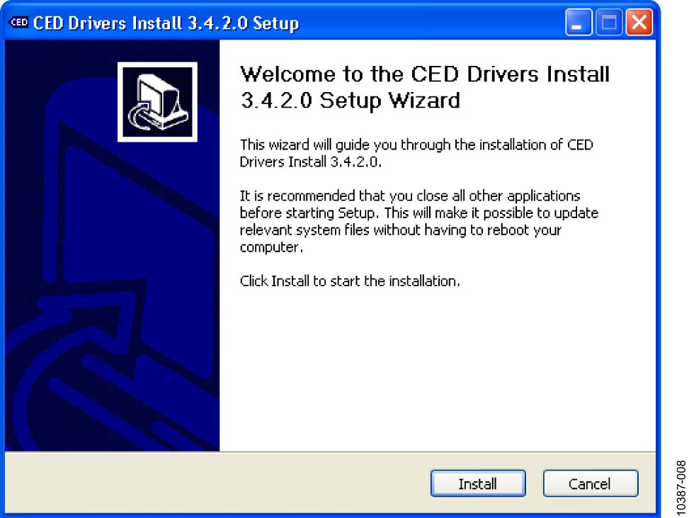
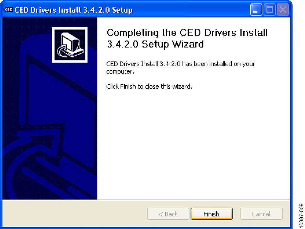
USB Drivers
The USB drivers install separately after the main software installation. Click Install when the driver installation wizard appears.
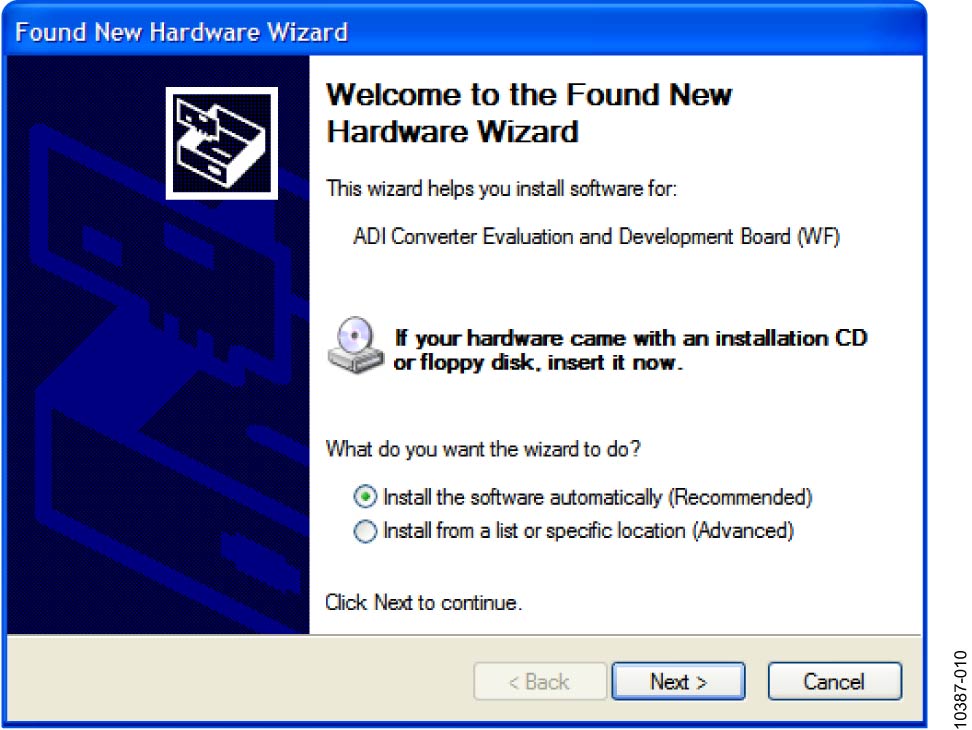
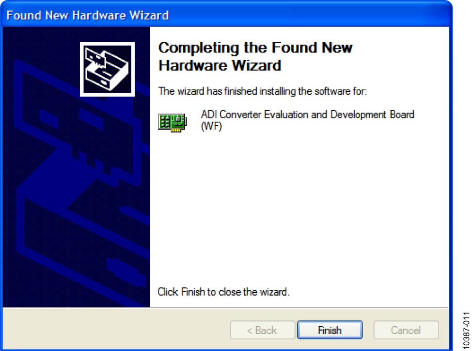
After connecting the EVAL-CED1Z via USB, the Found New Hardware Wizard initiates. When properly installed, the wizard confirms the evaluation board software is ready.
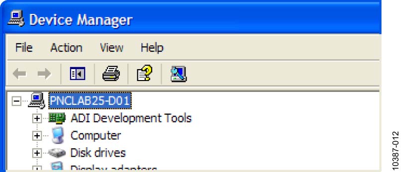
Verify the board appears in Device Manager under ADI Development Tools.
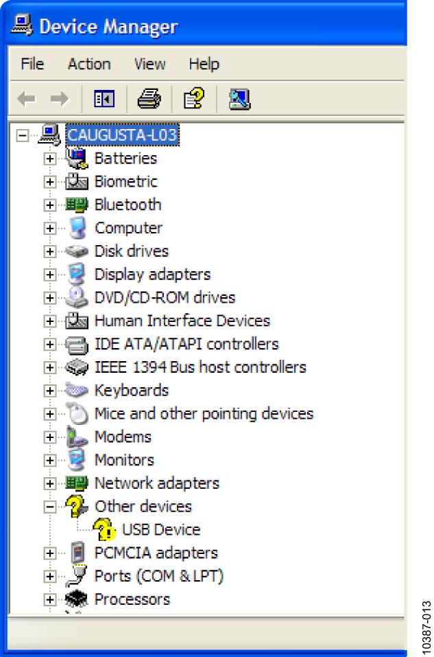
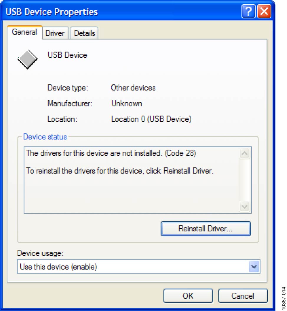
Troubleshooting the Installation
If the driver installation failed, Windows shows a question mark for “Other devices” in Device Manager. This is usually caused by non-administrator installation. Re-install as administrator with full privileges.
Running the Evaluation Software
The evaluation software performs:
Histogram for code transition noise (DC)
FFT for SNR, SINAD, THD, and SFDR
Decimation (digital filtering)
The software is located at:
C:\Program Files\Analog Devices\PulSAR ADC Evaluation Software\Eval PulSAR CED.exe
It is also available in the Start menu under Analog Devices PulSAR Evaluation Software.
Software Operation
Starting the software opens the Raw Data Capture window.
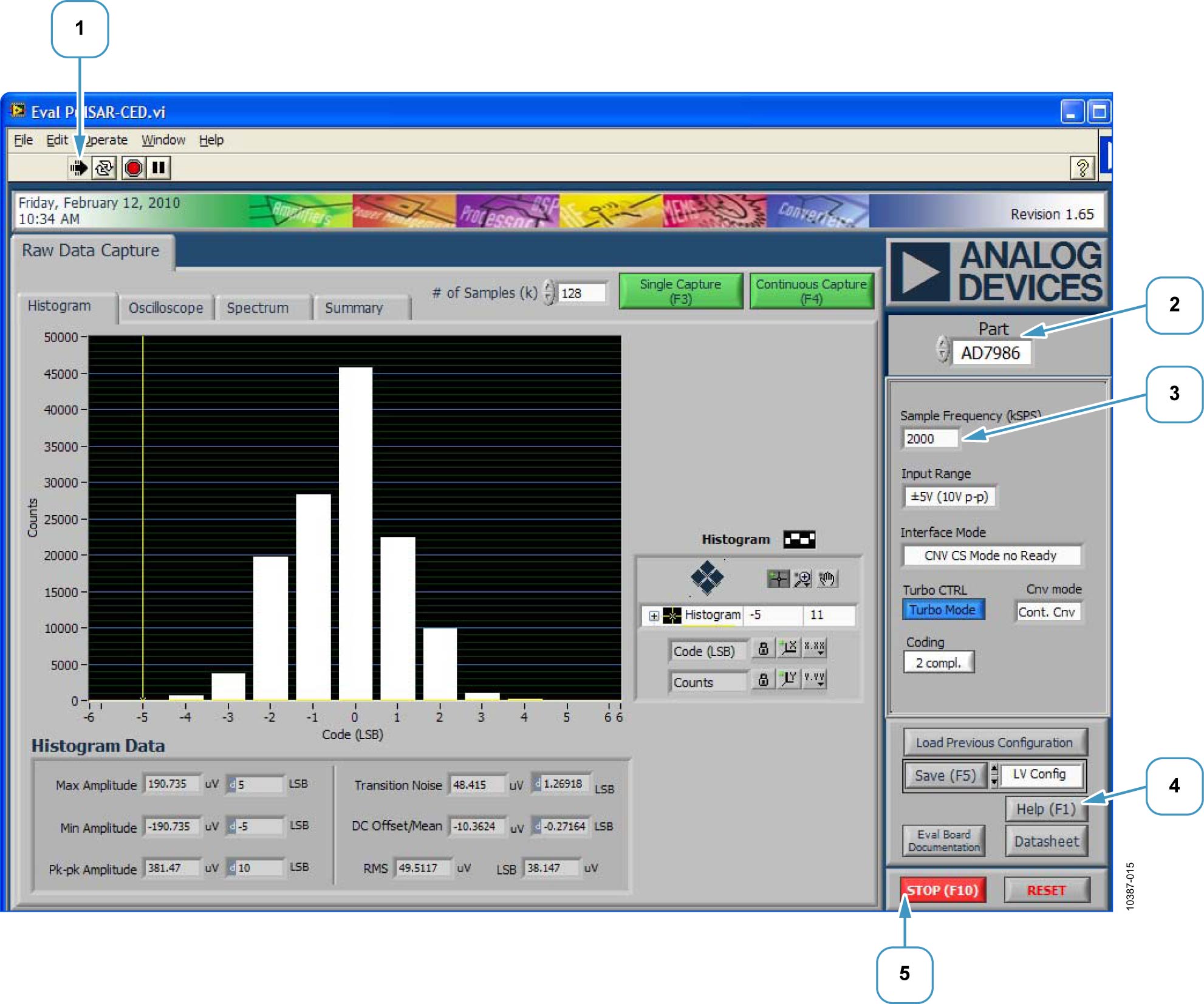
Click the arrow in the upper left corner to start.
Set the controls:
Sample Frequency: Enter rate in kHz (supports notation like “10k” for 10,000,000 Hz or “10 MSPS”).
Input Range: Select 4.096V or 5V for correct LSB display.
Interface Mode: Select Busy mode options.
Turbo CTRL: Select Turbo mode or normal mode.
CNV Mode: Select Continuous or burst conversion.
Coding: AD7986 uses “2 compl” (twos complement); AD7944/AD7985 use binary.
Control functions (top menu):
Save (F5): LV Config, HTML, or Spreadsheet options.
Stop (F10): Halt software.
RESET: Reset the CED capture board.
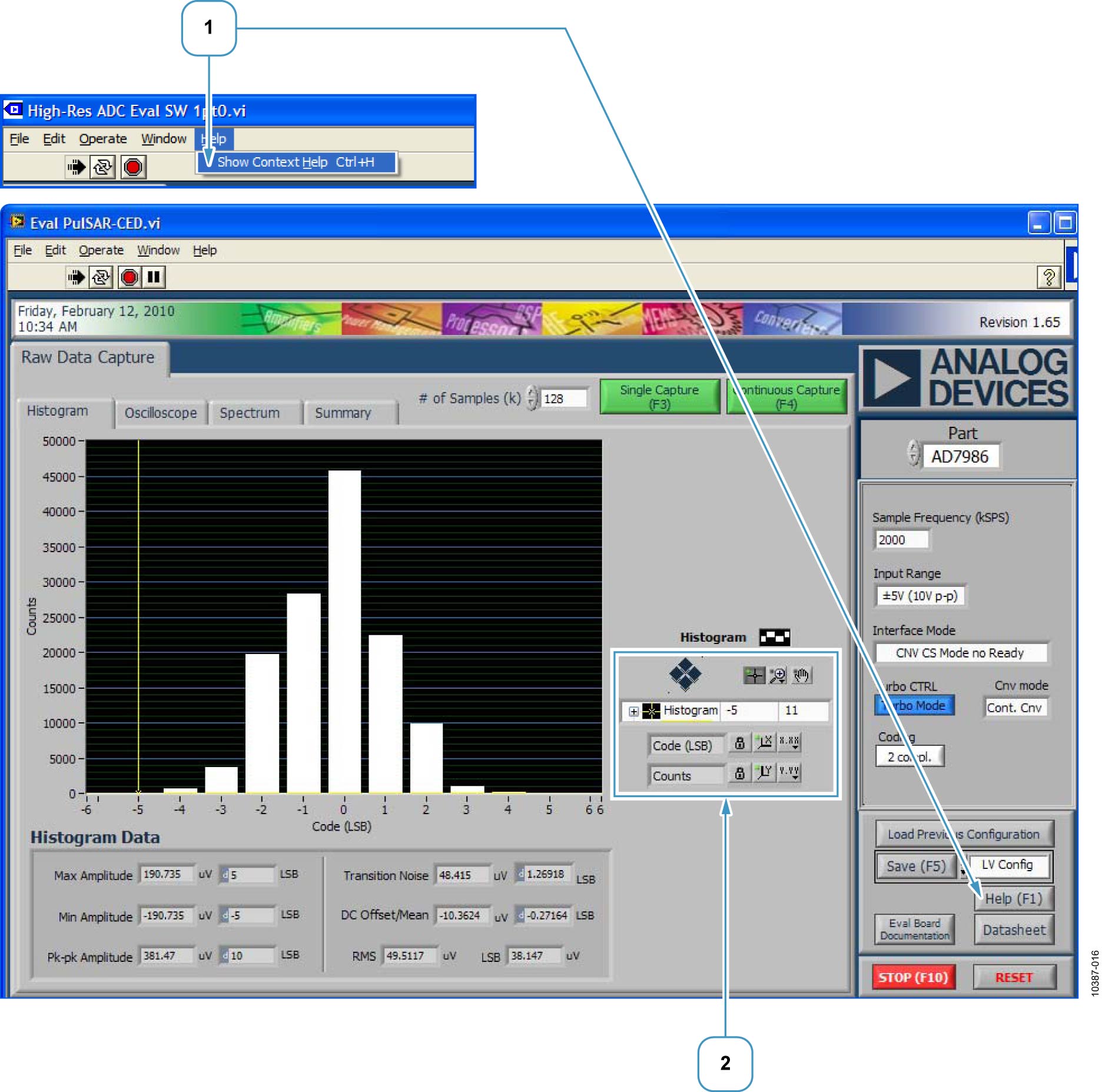
Context Help
Select Help > Show Context Help or press F1. Hovering over screen items displays context information.
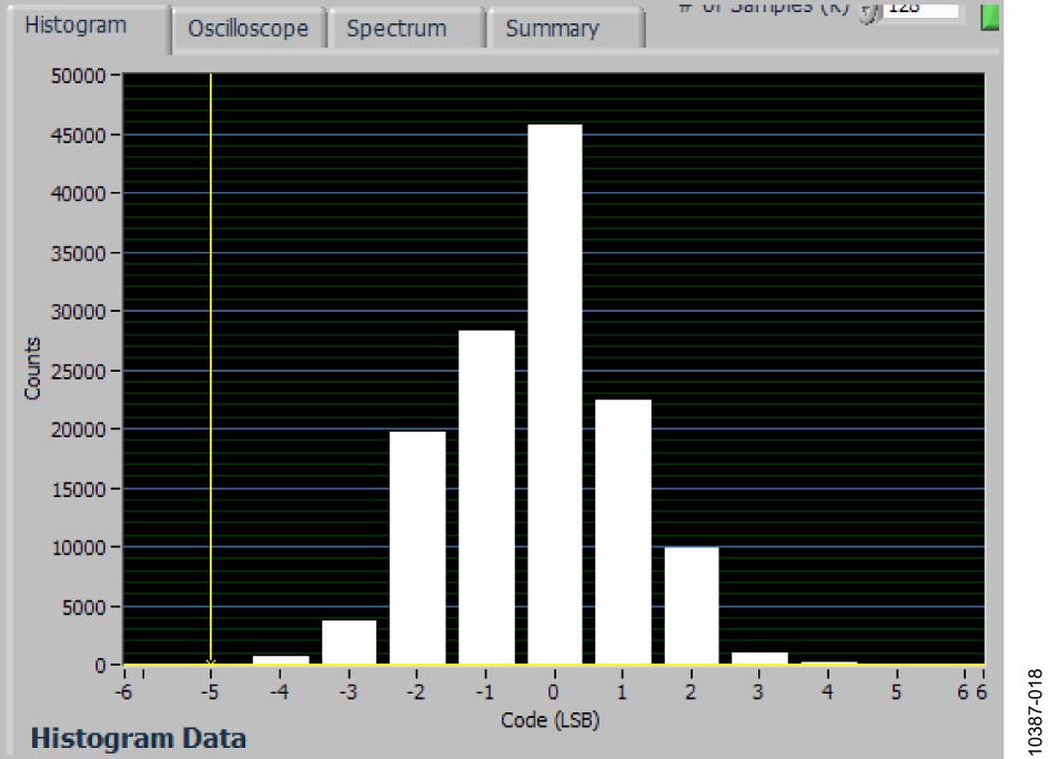
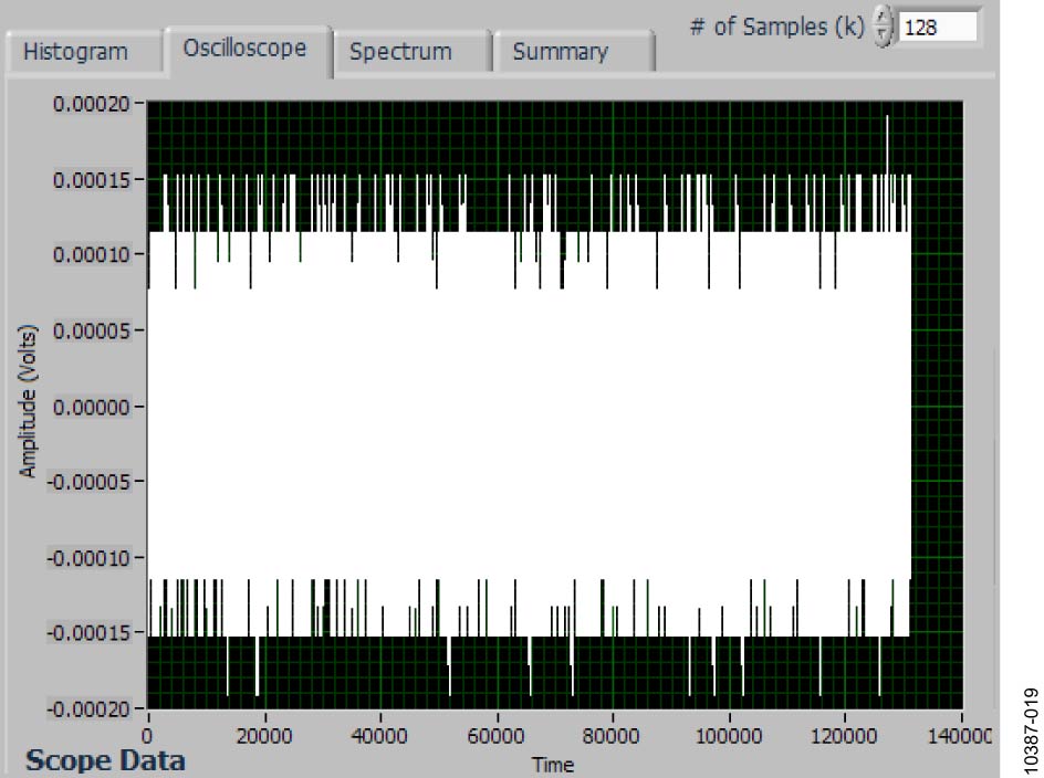
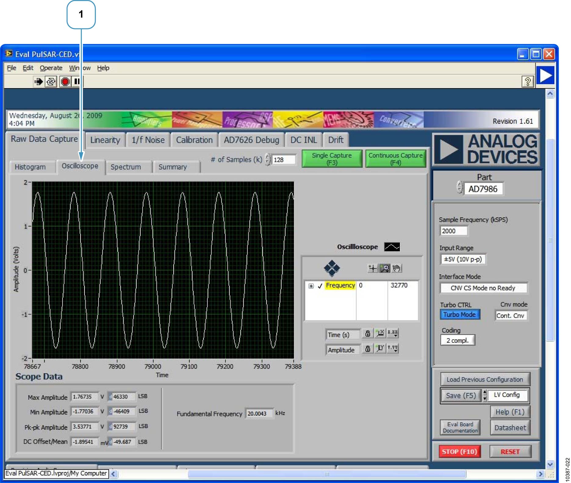
Histogram and Oscilloscope Charts
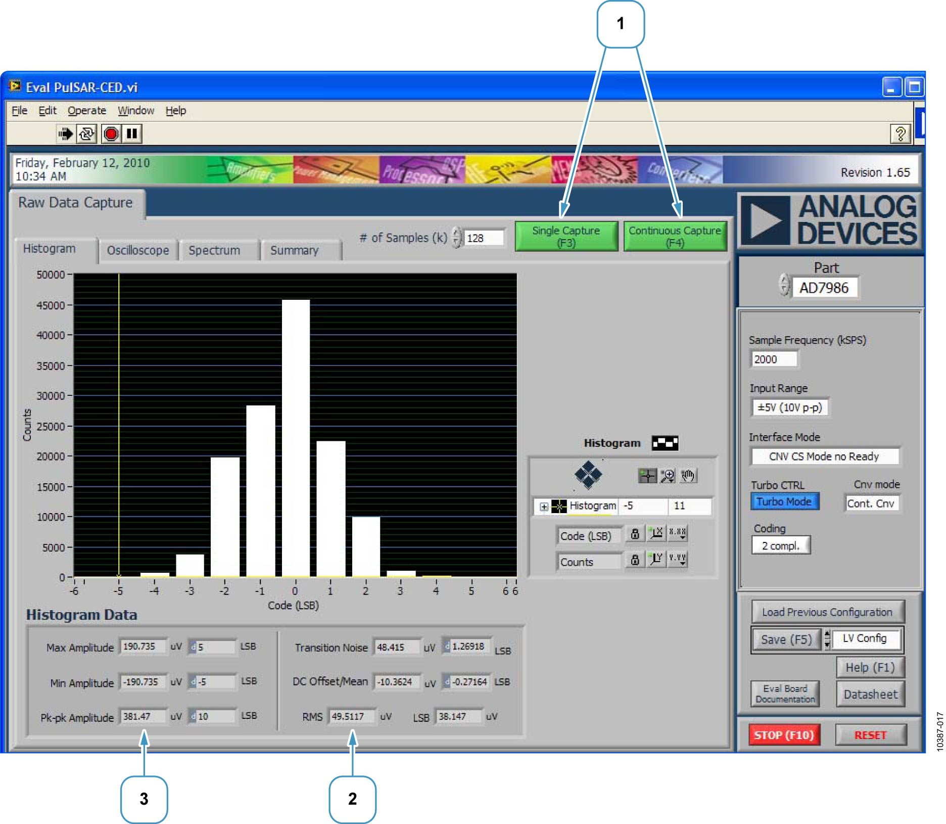
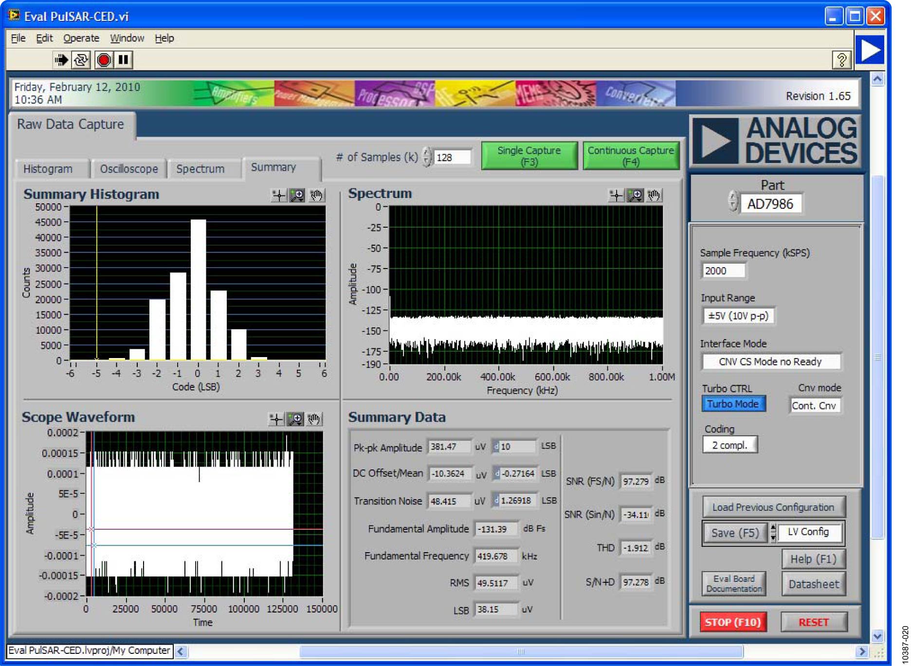
Use the buttons to select single or continuous data capture. Enter the sample count in the “# of Samples (k)” field. Statistics display in the Histogram Data section; graphics display in the chart area. Results can be viewed as histogram or oscilloscope via tab selection. The “Summary” tab shows both charts together.
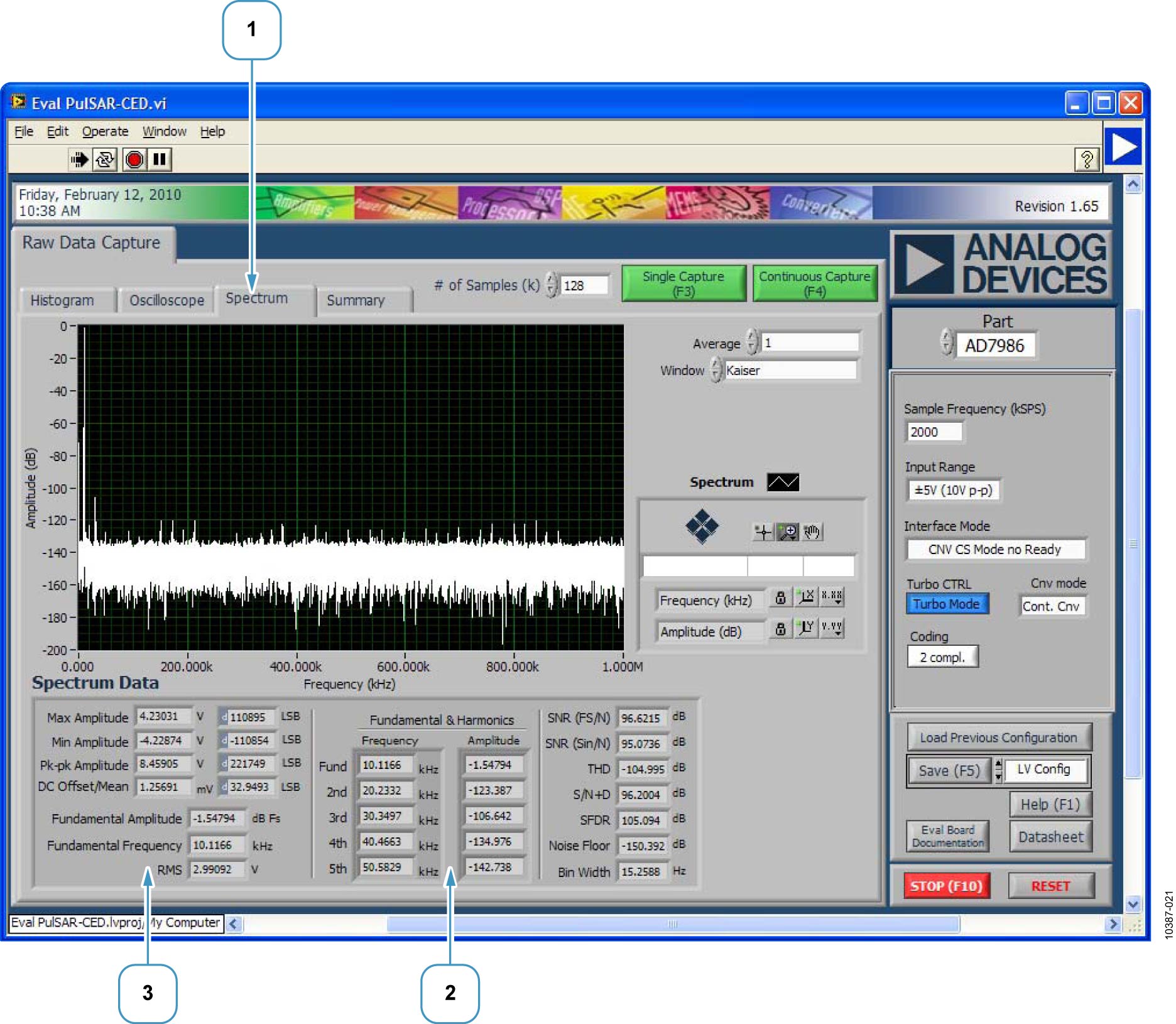
FFT Spectrum Data
Select the “Spectrum” tab in the Raw Data Capture window. The Spectrum Data section shows x-axis (frequency) and y-axis (magnitude) data.
Troubleshooting
Software Tips
Install the software from the CD or website before connecting the hardware.
Allow the full installation (two-part: software + drivers); a PC restart may be required.
Let the Found New Hardware Wizard complete when first plugging in the USB.
Verify board connection to the EVAL-CED1Z, daughter card connection, and Device Manager recognition.
Hardware Tips
If the software reads no data:
Verify the EVAL-CED1Z power and voltages on the P connectors.
Confirm signal source operation and expected signal output.
Probe the signal path points (driver amplifier inputs, ADC inputs).
For SNR performance issues:
Some sources require filtering; the board was tested with the AP-2322 analyzer/source.
Ensure the signal amplitude covers the full-scale ADC range.
Monitor the max/min amplitude or fundamental in the Spectrum tab.
Adjust the source for full-scale swing.
Design Resources
Complete design support files (schematics, Gerber files, bill of materials) and evaluation software are available for download from the respective evaluation board product pages on analog.com.