Clocking Architecture
The X-Band platform uses a sophisticated clocking architecture to maintain phase coherence across all 32 channels while providing flexibility for different applications and test configurations.
Overview
Proper clocking is critical for the X-Band platform’s performance, especially for beamforming applications where phase relationships between channels must be precisely maintained. The system provides multiple clocking options to accommodate different use cases.
Default MxFE Clocking Scheme
The default clocking scheme uses the AD9081’s on-chip PLL. The HMC7044 provides the reference into the chip, derived from the on-board VCXO crystal oscillator. An external reference signal can be applied to the HMC7044 via the EXT_HMCREF SMP-F connector if phase lock to external test equipment is required. No firmware or hardware changes are needed for this.
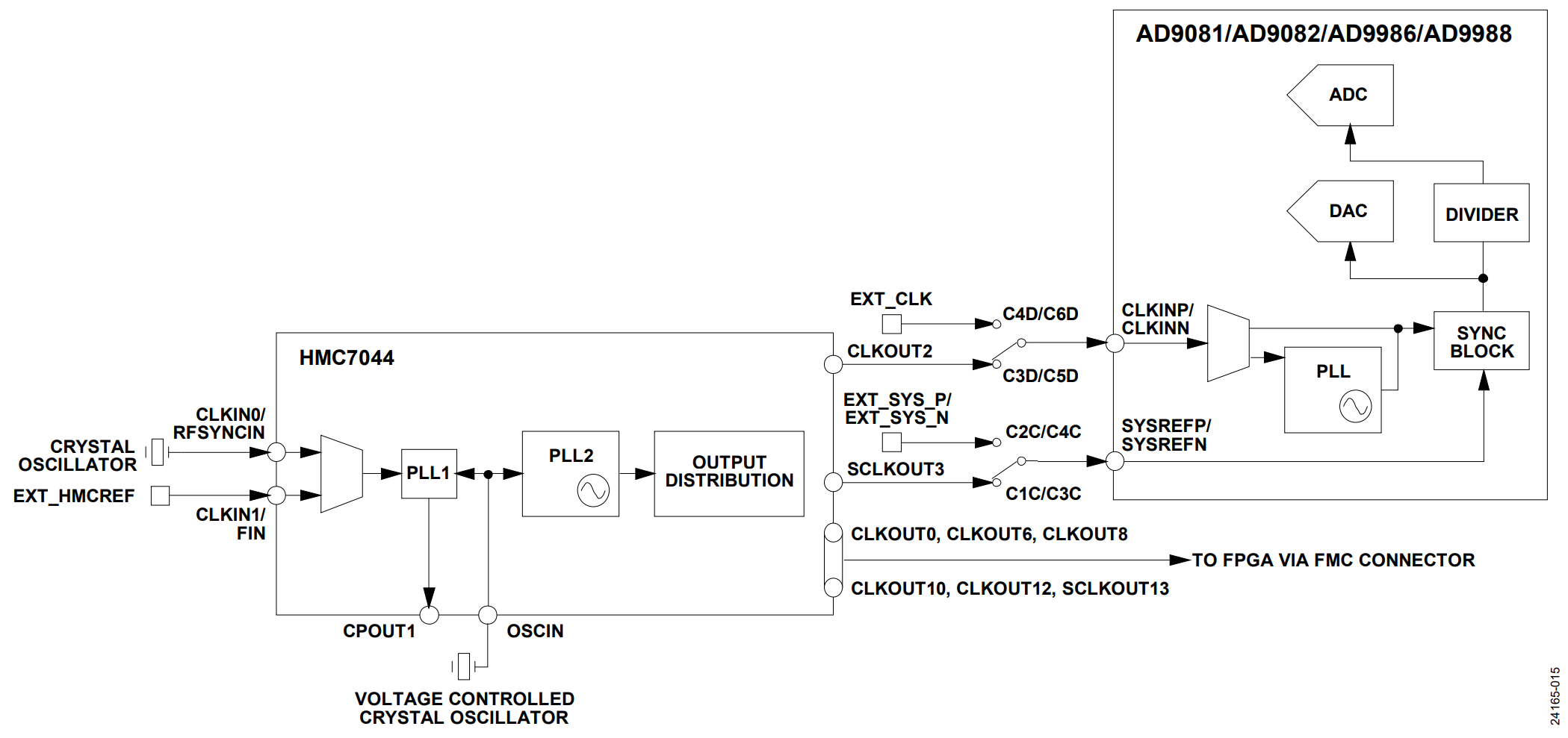
HMC7044 Clock Reference Priority
The firmware build HMC7044 reference clock priority is:
CLKIN1 (Highest priority)
CLKIN0
CLKIN2
CLKIN3 (Lowest priority)
Note
An external reference clock can be applied to the EXT_HMCREF SMP-F input without any firmware or hardware modifications. The HMC7044 will automatically select it based on the priority table.
Direct MxFE Clocking Option
The MxFE Evaluation Platform has provisions for directly driving the sampling clock of the MxFE data converter. An SMP-F plug is available at the EXT_CLK connector, which connects to an AC-coupling capacitor that is not populated by default.
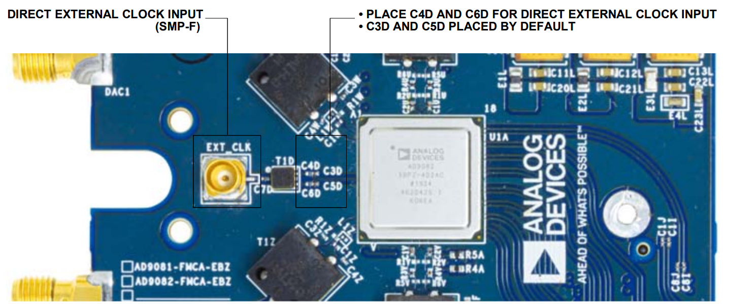
Hardware Modifications Required
SMP-F Ref Des |
Modification |
|---|---|
EXT_CLK |
Depopulate C3D/C5D, Populate C4D/C6D |
Warning
Direct clocking modifications should only be performed by experienced personnel. Improper modifications can damage the board or degrade performance.
XUD1A LO Architecture
The ADXUD1AEBZ provides flexible local oscillator (LO) generation options for frequency conversion.
Default External LO Configuration
The default LO configuration uses an external LO via SMA-F connector. The LO is common across all 4 up/down converter channels via an internal splitter network.
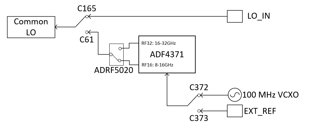
Input: External LO via
LO_INSMA-F connectorDistribution: Common LO split across all 4 channels
On-Board PLL: ADF4371 available as alternative (see below)
Reference: 100 MHz VCXO on-board, or external via
EXT_REF
On-Board PLL Configuration
The on-board ADF4371 PLL can be used in lieu of an external LO signal. The default ADF4371 reference clock is the on-board 100 MHz VCXO, but provisions are available to provide an external reference via a SMP-F connector.
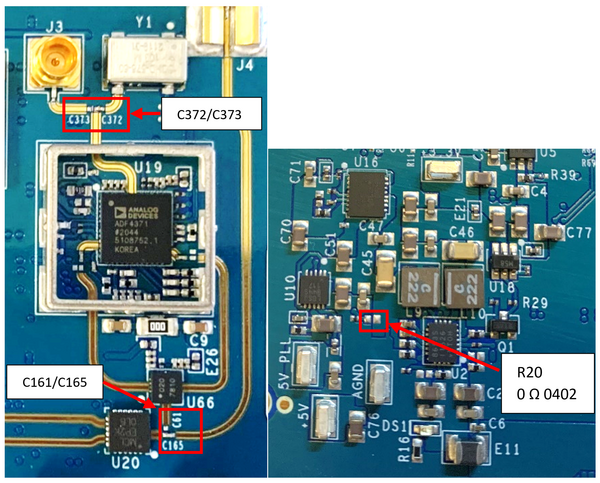
Hardware Modifications for Internal PLL
Implementation |
Modification |
|---|---|
ADF4371 Output |
Depopulate C165, Populate C61 |
ADF4371 External Reference |
Depopulate C372, Populate C373 |
ADF4371 +5V Enable |
Populate R20 with 0Ω 0402 resistor |