User Guide
Overview
The AD4170-4 Customer Evaluation Board User Guide provides comprehensive information about the EVAL-AD4170-4ARDZ evaluation kit and the AD4170-4 device. This guide covers hardware setup, configuration, software procedures, and practical applications for evaluating the device.
Hardware Setup
Block Diagram
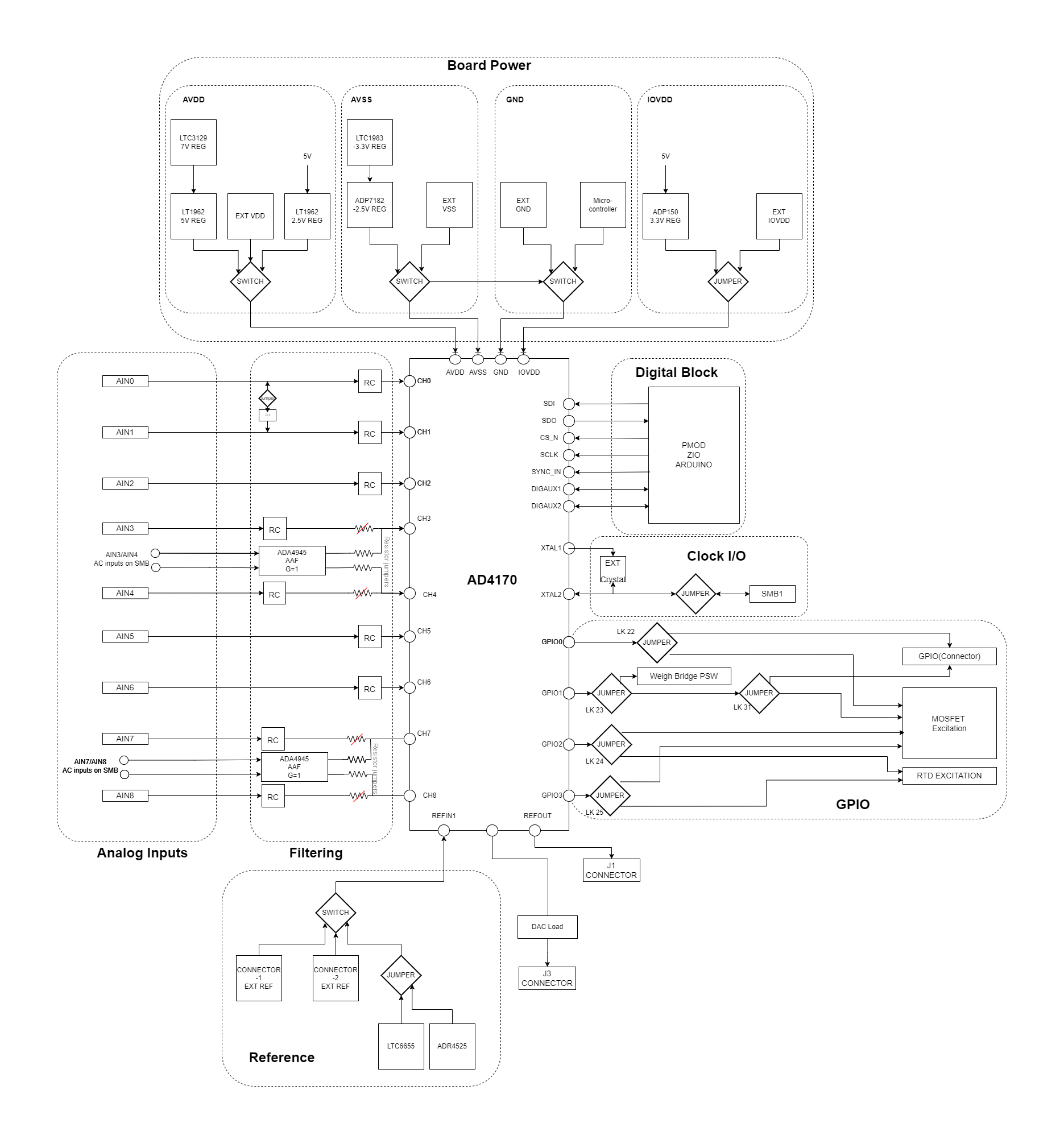
Connection Overview
The evaluation board connects to a compatible controller board through Arduino-compatible connectors, providing a flexible and standardized interface for signal routing and control.
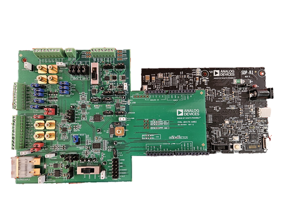
Figure 1 Example of evaluation board connected to the SDP-K1 controller board
Power Supply Configuration
Board Connections
The evaluation board features multiple connectors for signal input:
J1: Primary signal input connector
J2: Sensor excitation and bridge connections
J3: Additional sensor/digital signal connections
J4: GPIO and digital control
J5: Amplifier and external voltage supply
SMB connectors: Reference and clock inputs
Reference and Clock Options
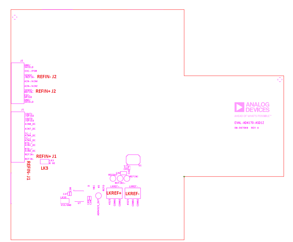
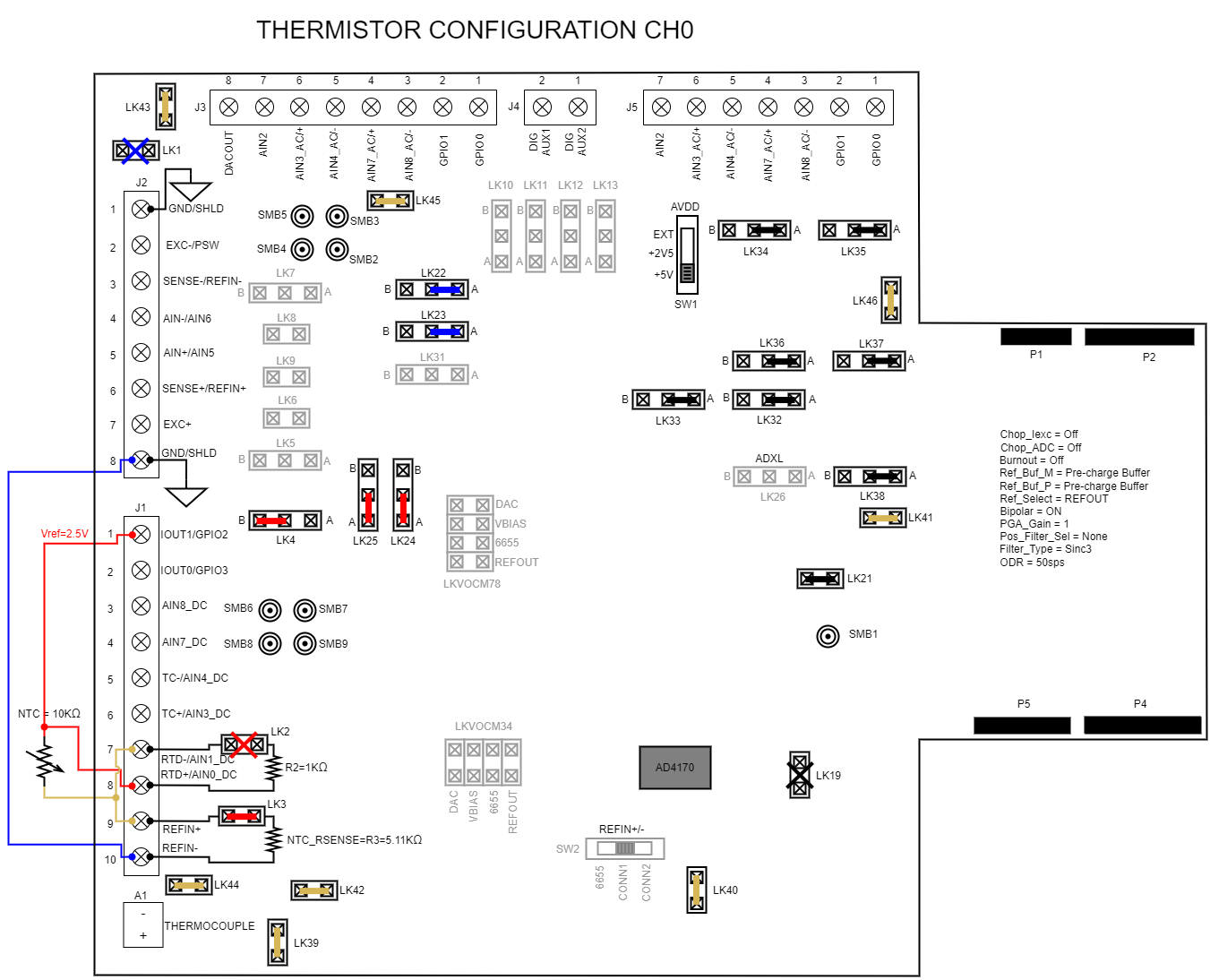
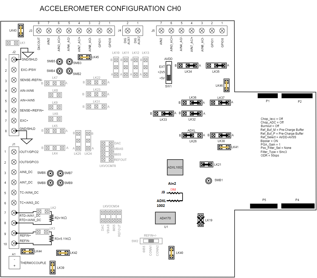
Hardware Link Configuration
The evaluation board uses configurable jumpers (links) to customize the hardware setup for different applications. The following table describes the available links:
Link Numbers |
Colour |
Default Position |
Description |
Rough Board Location |
|---|---|---|---|---|
LK1 |
Blue |
Inserted |
Noise Test. Channels AIN5 + AIN6 |
Right of J1 |
LK2 |
Red |
Inserted |
Thermocouple - Cold Junction Resistor Bypass |
Right of J1 |
LK3 |
Red |
Inserted |
Precision Reference Resistor Bypass |
Right of J1 |
LK4 |
Red |
A |
Pos A: GPIO 1 (IOUT1) to J1 Pos B: REFOUT |
Right of J1 |
LK5 |
Blue |
B |
Wire Bridge EXC+ select: Pos A: MOSFET+ Pos B: AVDD |
Right of J2 (EXC+) |
LK6 |
Blue |
Uninserted |
Short EXC+/REFIN+: Pos Inserted = 4 Wire Bridge |
Right of J2 (4/6 wire) |
LK7 |
Blue |
B |
Wire Bridge EXC- select: Pos A: MOSFET- Pos B: Power Switch (GPIO1) |
Right of J2 (EXC-) |
LK8 |
Blue |
Uninserted |
Short EXC-/AVSS: Pos Inserted = 4 Wire Bridge |
Right of J2 (EXC-) |
LK9 |
Blue |
Uninserted |
Short EXC-/REFIN-: Pos Inserted = 4 Wire Bridge |
Right of J2 (4/6 wire) |
LK10 |
Black |
A |
ADA4595-1 AIN3+ AIN4. AVDD select. Pos A: Internal AVDD Pos B: External AVDD |
Below of J5 (AMP34) |
LK11 |
Black |
A |
ADA4595-1 AIN3+ AIN4. AVSS select. Pos A: Internal AVSS Pos B: External AVSS |
Below of J5 (AMP34) |
LK12 |
Black |
A |
ADA4595-1 AIN7+ AIN8. AVDD select. Pos A: Internal AVDD Pos B: External AVDD |
Below of J5 (AMP78) |
LK13 |
Black |
A |
ADA4595-1 AIN7+ AIN8. AVSS select. Pos A: Internal AVSS Pos B: External AVSS |
Below of J5 (AMP78) |
LK14 |
N/A |
DNI |
SCP connect AC amplifier external AVSS and Ground |
Left of J5 |
LK15 |
N/A |
DNI |
SCP connect external AVSS and Ground |
Right of J5 |
LK16 |
N/A |
DNI |
SCP connect external AVDD and Ground |
Right of J5 |
LK17 |
N/A |
DNI |
SCP connect external IOVDD and Ground |
Right of J5 |
LK18 |
N/A |
DNI |
SCP connect AC amplifier external AVDD and Ground |
Left of J5 |
LK19 |
Black |
Uninserted |
XTAL2 to Digital connector |
Above PMOD (P6) |
LK20 |
Black |
A |
External VREF LTC6655 |
Right to J1 |
LK21 |
Black |
Inserted |
Inserted: External crystal Uninserted External clock |
Above SMB1 (Right) |
LK22 |
Blue |
A |
GPIO 0: Pos A: To Connector J4 Pos B: Mosfet |
Below J4 |
LK23 |
Blue |
A |
GPIO 1: Pos A: To Connector J4/J2 (LK31) Pos B: Mosfet |
Below J4 |
LK24 |
Red |
A |
GPIO 2: Pos A: To Connector J1 Pos B: Mosfet |
Right of J2 |
LK25 |
Red |
A |
GPIO 3: Pos A: To Connector J1 Pos B: Mosfet |
Right of J2 |
LK26 |
Black |
A |
ADXL1002 Test Pos A: Test Pos B:Standard |
Below IOVDD LED (midle right) |
LK31 |
Blue |
A |
GPIO1 Connector select. Pos A: J2 (Power Switch) Pos B: J3 |
Below J4 |
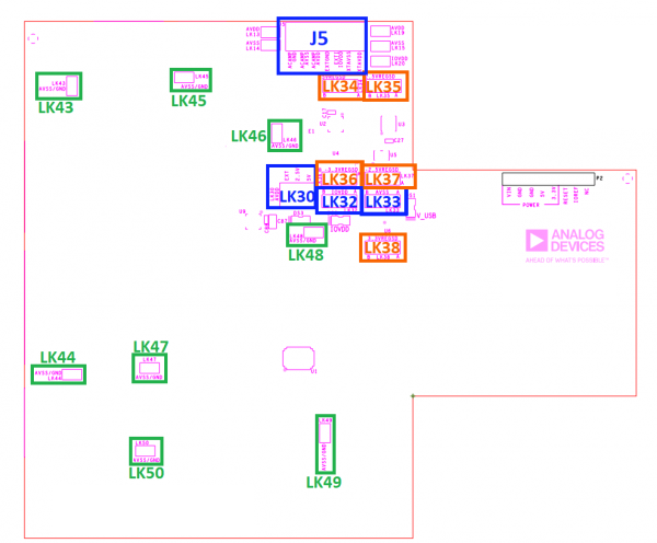
LK32 |
Black |
A |
IOVDD select. Pos A: 3.3V Pos B: EXT |
Below J5 (near IOVDD LED) |
LK33 |
Black |
A |
LT1962-5 power down Pos A: On |
Below J5 |
LK34 |
Black |
A |
LTC3129 power down Pos A: On |
Below J5 |
LK35 |
Black |
A |
LT1962-2.5 power down Pos A: On |
Below J5 |
LK36 |
Black |
A |
LTC1983 power down Pos A: On |
Below J5 |
LK37 |
Black |
A |
ADP7182 power down Pos A: On |
Below J5 |
LK38 |
Black |
A |
ADP150 power down Pos A: On |
Below J5 |
LK39 |
Grey |
Inserted |
AVSS GND short |
Top Left |
LK40 |
Grey |
Inserted |
AVSS GND short |
Above Thermocouple Connection |
LK41 |
Grey |
Inserted |
AVSS GND short |
Below J4 |
LK42 |
Grey |
Inserted |
AVSS GND short |
Below J5 |
LK43 |
Grey |
Inserted |
AVSS GND short |
Right of J1 |
LK44 |
Grey |
Inserted |
AVSS GND short |
Below J5 (near AVDD LED) |
LK45 |
Grey |
Inserted |
AVSS GND short |
Left of PMOD (P6) |
LK46 |
Grey |
Inserted |
AVSS GND short |
Right of Thermocouple Connection |
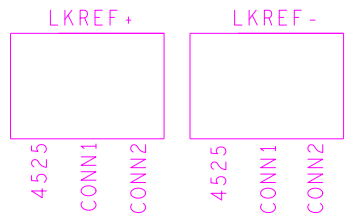
LKVOCM34 |
Black |
4525 |
VOCM ADA4945-1 Pos A: DACOUT Pos B: VBIAS Pos C: ADR4525 Pos D: REFOUT |
Right of Thermocouple Connection |
LKVOCM78 |
Black |
4525 |
VOCM ADA4945-1 Pos A: DACOUT Pos B: VBIAS Pos C: ADR4525 Pos D: REFOUT |
Middle of board |
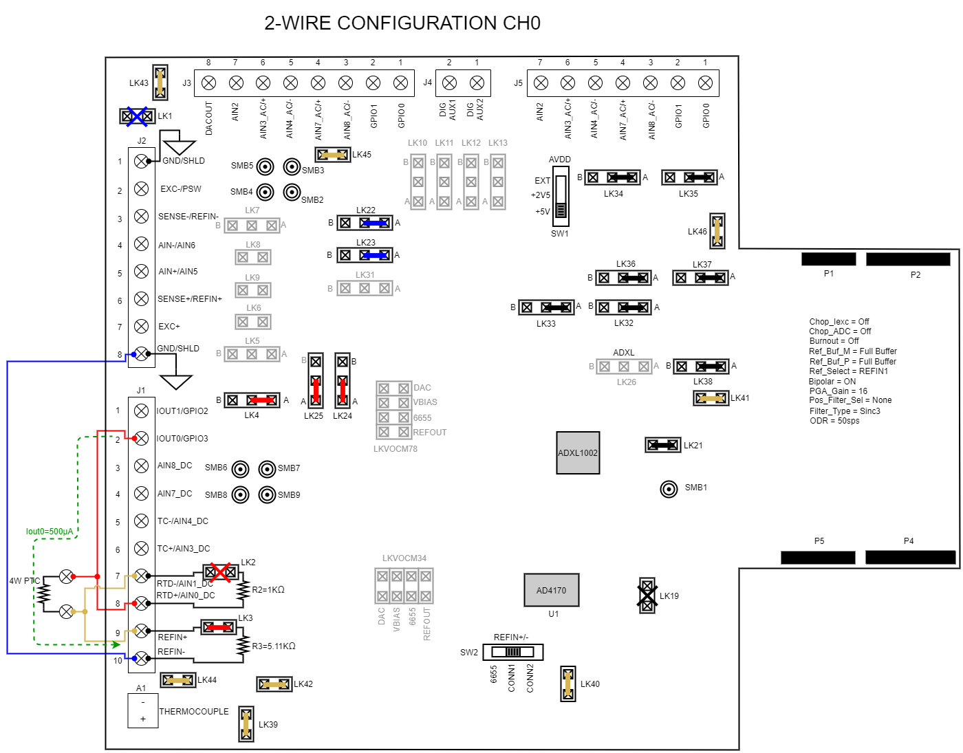
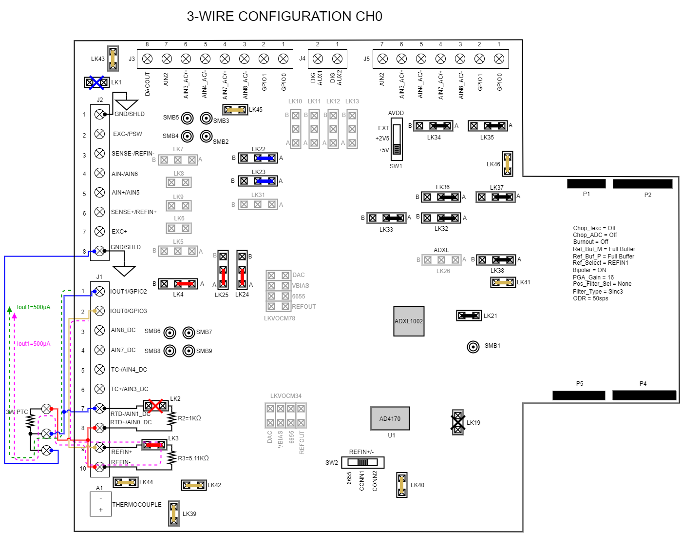
Sensor Configuration Examples
The AD4170-4 evaluation board supports multiple sensor types through flexible input configuration.
2-Wire Configuration (RTD)
3-Wire Configuration (RTD)
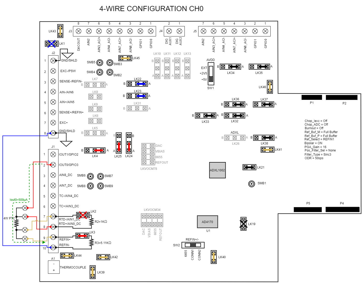
4-Wire Configuration
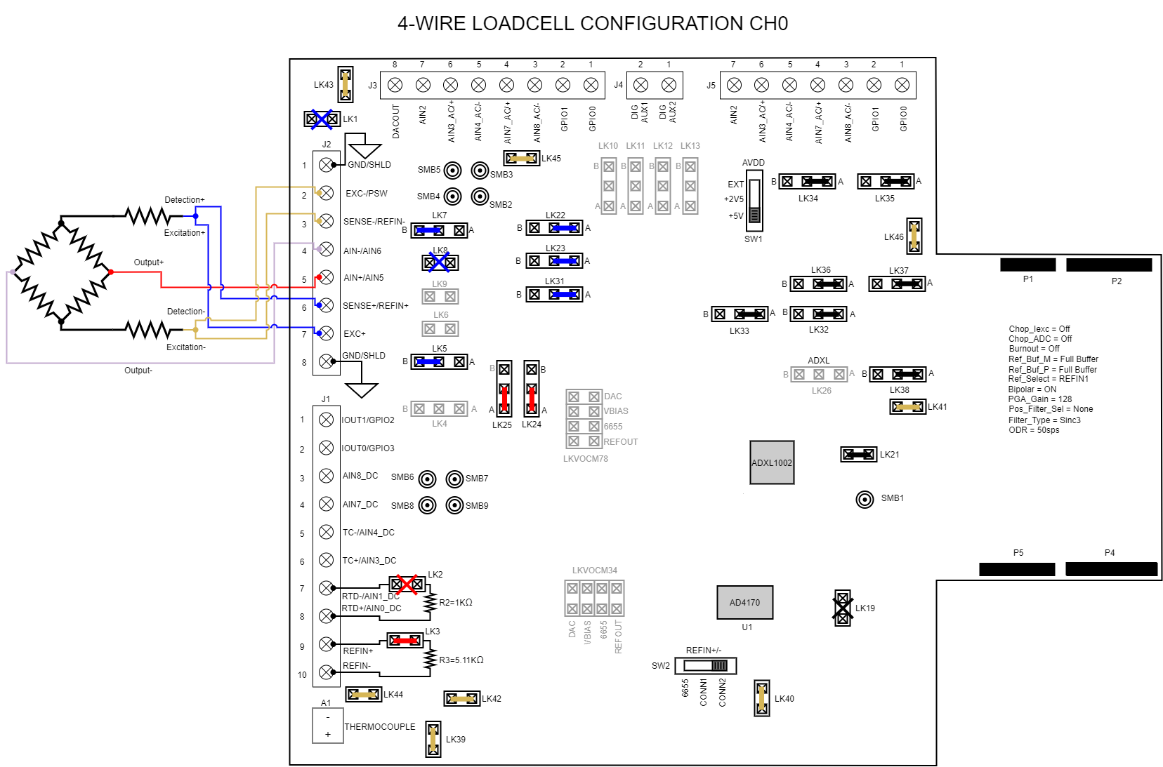
4-Wire Load Cell - DC Configuration
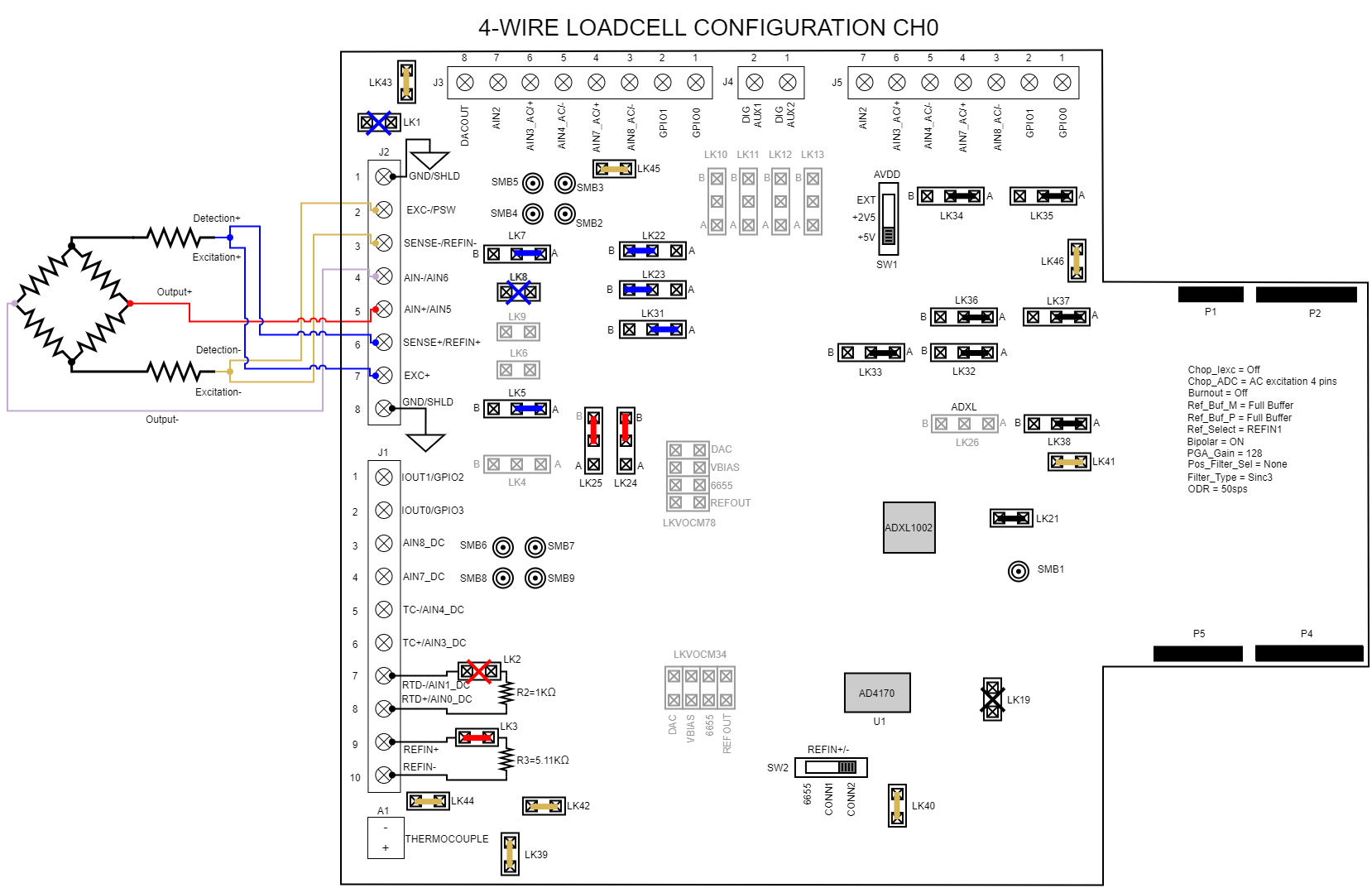
4-Wire Load Cell - AC Configuration
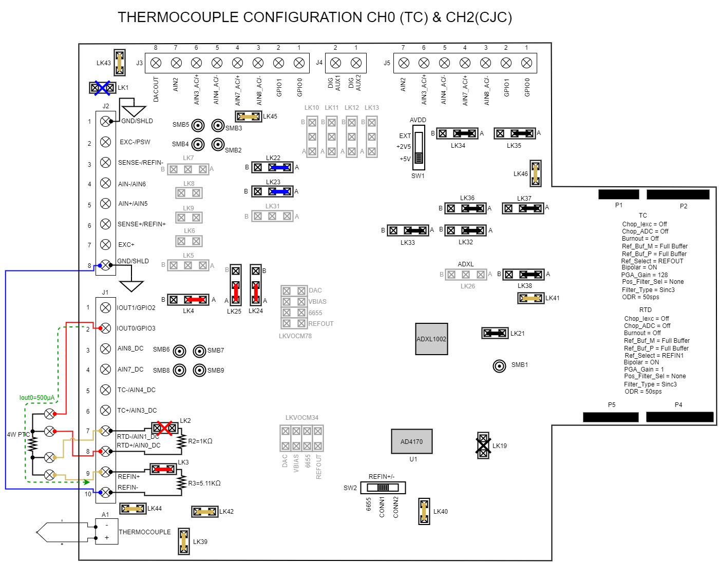
Thermocouple Configuration
RTD Thermistor Configuration
Accelerometer Configuration
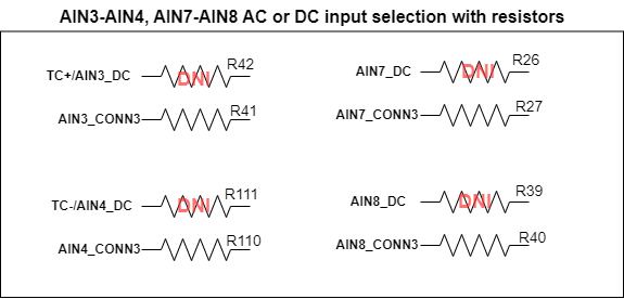
AC/DC Selection for Channels
For AC or DC input selection on channels AIN3-AIN4 and AIN7-AIN8, modify the resistor jumpers according to the table below:
AC/DC input |
CH3-CH4 |
CH7-CH8 |
AC input |
R41, R110 |
R27, R40 |
DC input |
R42, R111 |
R26,R39 |
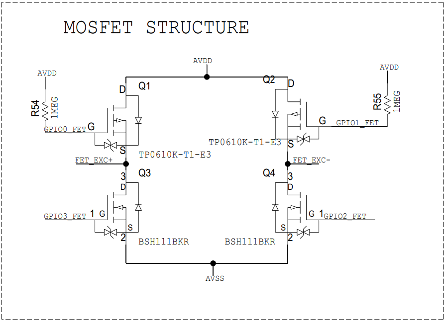
MOSFET Circuit Configuration