EVAL-AD7193-ASDZ Hardware Guide
Set-up Procedures
After following the instructions in the Software Procedures section, set up the evaluation and SDP boards as detailed in this section.
Warning
The evaluation software and drivers must be installed before connecting the EVAL-AD7193-ASDZ evaluation board and EVAL-SDP-CB1Z board to the USB port of the PC to ensure the PC correctly recognizes the evaluation system.
Connect the EVAL-AD7193-ASDZ to the controller board
Option A: Connect the EVAL-AD7193-ASDZ to the EVAL-SDP-CK1Z
Using the 120 pin connector
Screw the two boards together using the plastic screw-washer set included in the evaluation board kit to ensure that the boards are connected firmly together.
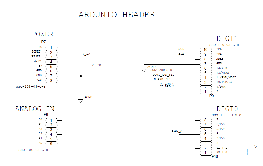
Using the Arduino Connectors
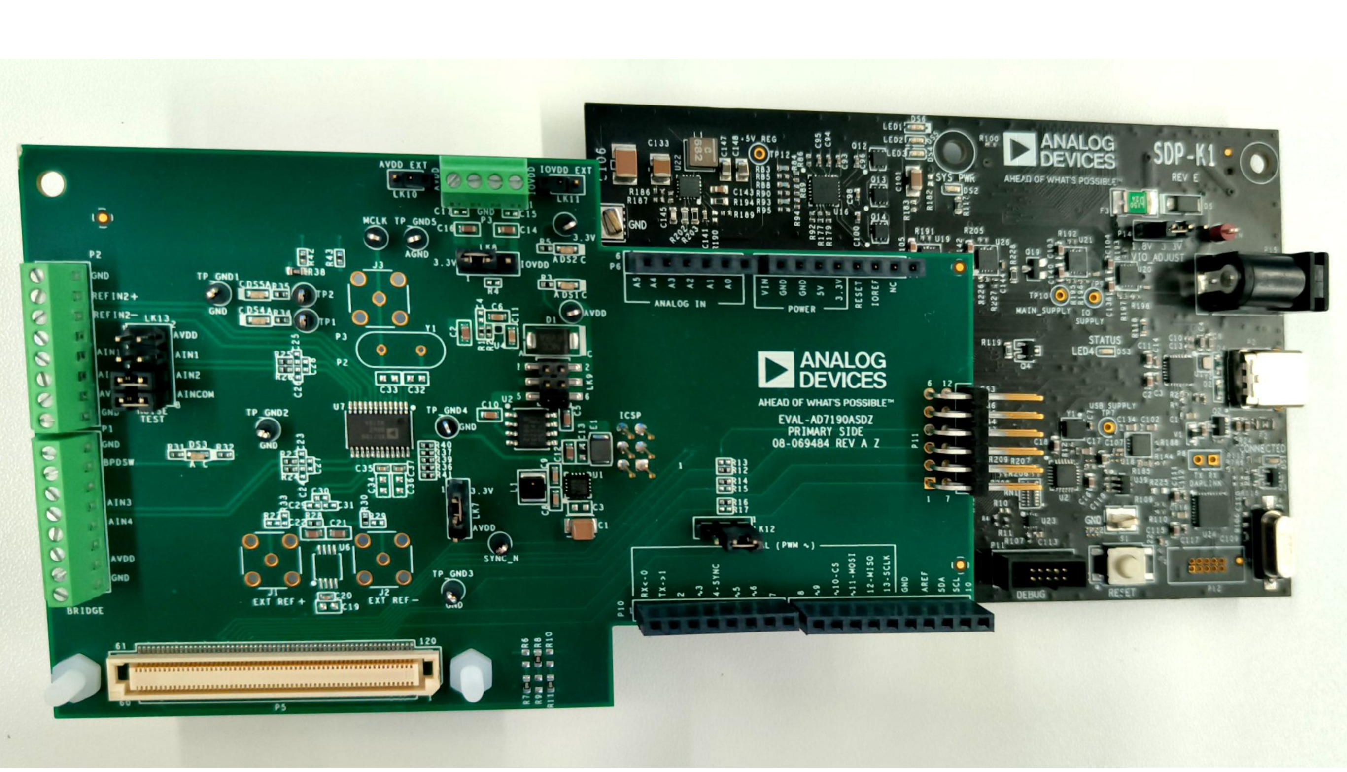
Option B: Connect the EVAL-AD7193-ASDZ to the EVAL-SDP-CB1Z
Using the 120 pin connector
Screw the two boards together using the plastic screw-washer set included in the evaluation board kit to ensure that the boards are connected firmly together.
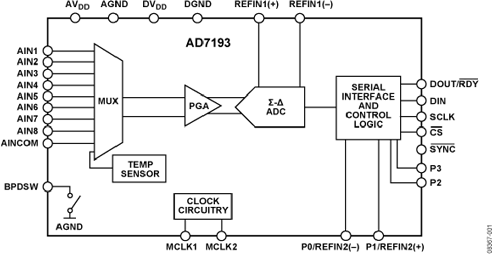
Block Diagram
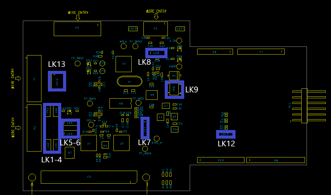
Hardware Link Options
Link Numbers |
Colour |
Default Position |
Description |
Rough Board Location |
|---|---|---|---|---|
LK1 |
Black |
Uninserted |
REFIN+ to AVDD/EXC |
Right of LK2 |
LK2 |
Black |
Inserted |
AVDD to AVDD/EXC For Brdige Connection |
Right of connector P3 |
LK3 |
Black |
Uninserted |
GND to PSW/EXC For Bridge Connection |
Right of connector P3 |
LK4 |
Black |
Uninserted |
REFIN- to PSW/EXC For Bridge Connection |
Right of LK3 |
LK5 |
Black |
A |
REFIN1- selction between P2 and P3 connectors |
Above LK6 |
LK6 |
Black |
A |
REFIN1+ selction between P2 and P3 connectors |
Above U7 |
LK7 |
Black |
A |
DVDD selection Pos A: 3.3V supply Pos B: AVDD |
Right of J2 |
LK8 |
Black |
A |
IOVDD selection Pos A: 3.3V LDO Pos B: External IOVDD |
Near connector P4 |
LK9 |
Black |
C |
AVDD selection Pos A: 3.3V LDO Pos B: External AVDD Pos C: 5V LDO |
Right of U6 |
LK12 |
Black |
A |
Chip Select Selection Pos A: CS_ARD_1 Pos B: CS_ARD_2 |
On Arduino shield |
LK13 |
Black |
Uninserted |
To Enable Low Noise Test |
Right of P1 |
On Board Connections
Bridge Connections
Connector P3: DC (Analog Input)
Functionality:
Bridge Connection
Connection |
Function |
|---|---|
1 |
Ground/Sheild |
2 |
Excitation- |
3 |
External Reference - |
4 |
AIN 7 with DC filtering |
5 |
AIN 8 with DC filtering |
6 |
External Reference + |
7 |
Excitation+ |
8 |
Ground/Sheild |
Link Lk13: Low Noise Test Circuitry
Functionality:
Low Noise Test
-ALL INSERTED
Connection |
Function |
|---|---|
1-2 |
AVDD |
3-4 |
AIN1 |
5-6 |
AIN2 |
External Powers
Connector |
Function |
|---|---|
P4 Pin 1-2 |
External IOVDD connection |
P4 Pin 3-4 |
External AVDD connection |
LK10 |
External AVDD connection for SCP Boards |
LK11 |
External IOVDD connection for SCP Boards |
Digital Connectors
SDP 120 Pin Connector P5 |
Function |
Arduino connector P6,P7,P9,P10 |
|---|---|---|
3,4 |
GND |
P7-6,P7-7 |
5 |
V_USB |
P7-5 |
6,11,17,23,28,36,40,46,52 |
GND |
P9-7 |
56 |
EEPROM_A0 |
|
58,63,69,75 |
GND |
|
78 |
SYNC_IN |
P10-5 |
79 |
SCL |
P10-10 |
80 |
SDA |
P10-9 |
81 |
GND |
|
82 |
SCLK |
P10-6 |
83 |
SDO/miso |
P10-5 |
84 |
SDI/mosi |
P10-4 |
85 |
CS_N |
P9-3,P9-2 |
86,93,98,109,115 |
GND |
|
116 |
VIO |
P7-2 |
117,118 |
GND |
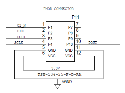
Pmod Connector P11
Connection |
Function |
Connection |
Function |
|---|---|---|---|
1 |
CS_N |
7 |
|
2 |
DIN |
8 |
|
3 |
DOUT |
9 |
|
4 |
SCLK |
10 |
|
5 |
GND |
11 |
GND |
6 |
IOVDD |
12 |
IOVDD |
SMB Connections
There are 3 SMB connections on the board. To allow clock signals and reference into the board.
J1 Provides option for External Reference+
J2 Provides option for External Reference-
J3 Brings external MCLK to the AD7193
Power Supplies
The evaluation board receives power through the controller board when connected to the PC via USB. Linear regulators generate the required power supply levels from the applied USB voltage.
AVDD (LK9) selection
DVDD (LK7) selection
3.3V supply (DEFAULT)
3.3V supplies DVDD
AVDD
AVDD connected to DVDD
IOVDD (LK8) selection
3.3V supply (DEFAULT)
3.3V regulator supplies IOVDD ADP150
External IOVDD
Connections on Connector P4
V_IO from SDP
R38 to be mounted
Serial Interface
There are four primary signals: CS, SCLK, SDI, and SDO/RDY (all are inputs, except for SDO/RDY, which is an output).
Serial communication options
SDP-B board and the respective 120 pin SDP connector.
When using the SDP-B connection (120 pin) The evaluation board connects via the serial peripheral interface (SPI) to the Blackfin® ADSP-BF527 on the SDP-B board.
Arduino connection SDP-K1
Pmod connector
Standalone mode
Reference Options
DEFAULT ADR4525 On Board external reference on REFIN1+
LTC6655LN-2.5/LTC6655LN-4.096 On Board external reference on REFIN+
Option to use ultra low noise reference
External Reference on REFIN1+ Connector J1
AVDD as Reference via R25
External reference can be supplied on P1-1 and P1-2 for REFIN2+ and REFIN2-
Selecting the reference source:
Software
Board should be correctly connected to ACE
Option A: Open AD7193 memory map
Search for the Configuration register
Set the REFSEL[] to the desired reference source by using these bits:
REFSEL[0]: External reference applied between REFIN1(+) and REFIN1(−).
REFSEL[1]: External reference applied between P1/REFIN2(+) and P0/REFIN2(-) pins.
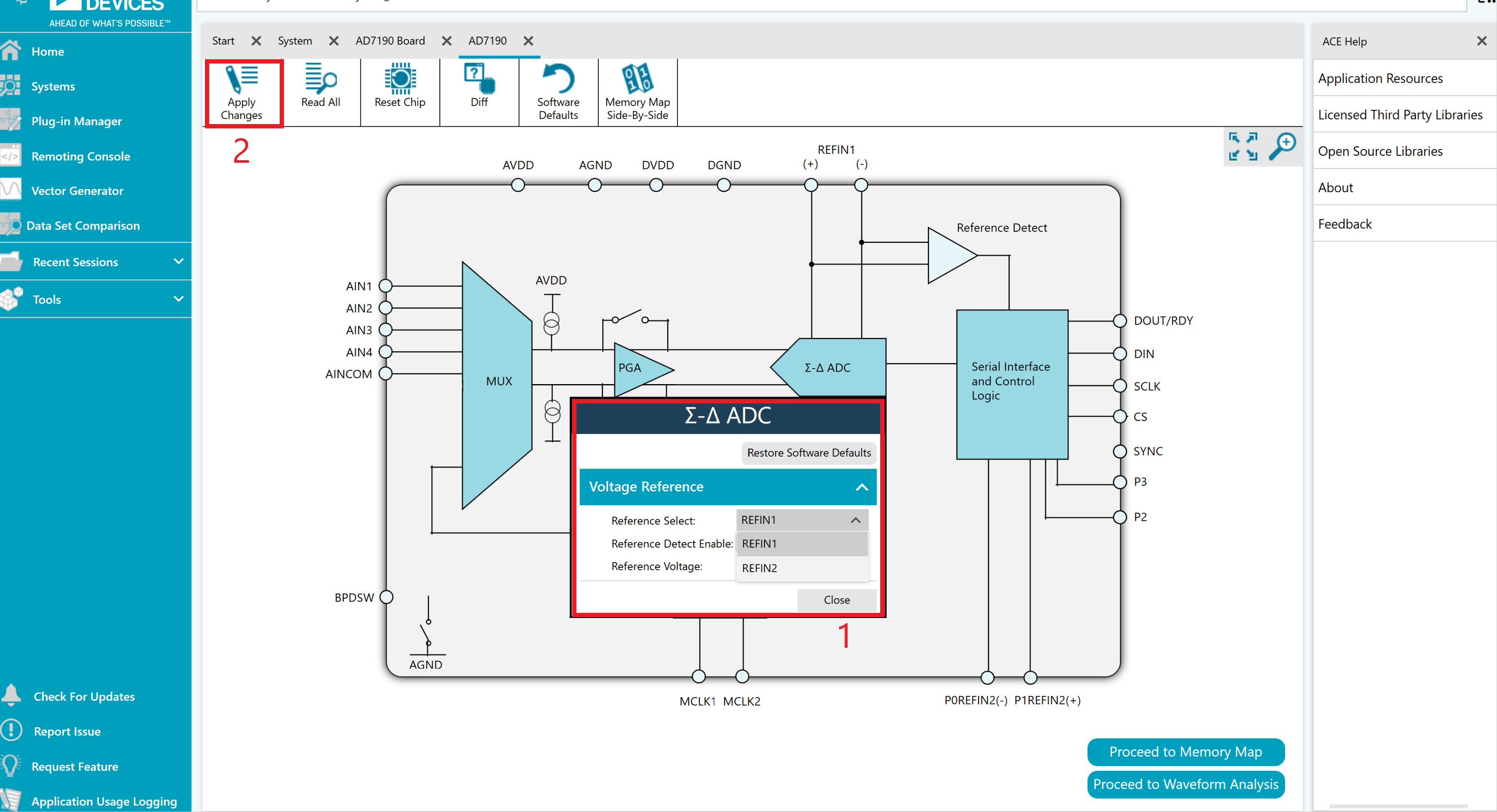
Option B: Open AD7193 Chip View
Right click on ADC block
Select Reference Source from the Reference Select option given as highlighted(1) below in the picture.
Click on Apply Changes as highlighted(2) below.
GPIOs
The General purpose inout pins are powered by AVDD/AVSS. They can be used to provide AC-Excitation signals for AC-Excited sensors, using 2 or 4 outputs. Can be used to automatically control an external multiplexer. Other optional functions include Current Source outputs , 2nd Reference input, Power-down switch.
GPIO |
Bit Name |
Functionality |
|---|---|---|
BPDSW |
BPDSW |
Bridge power-down switch |
P3 |
P3DAT |
Digital Output P3 |
P2 |
P2DAT |
Digital Output P2 |
P1 |
P1DAT |
Digital Output P1/REFIN2+ |
P0 |
P0DAT |
Digital Output P0/REFIN2- |
Evaluation board Connections and Functionality
The evaluation board highlights the functionality of the GPIOs
BPDSW
Available on the P1 connector.
Used as a Power Switch for Wire Bridge applications
P0/REFIN2-
Available on the P1 connector.
Also used as secondary reference option.
P1/REFIN2+
Available on the P1 connector.
Also used as secondary reference option.
Design and Integration Files
Schematics, layout files, and bill of materials are available on the EVAL-AD7193ASDZ product page.