ADXUD1A Up/Down Converter
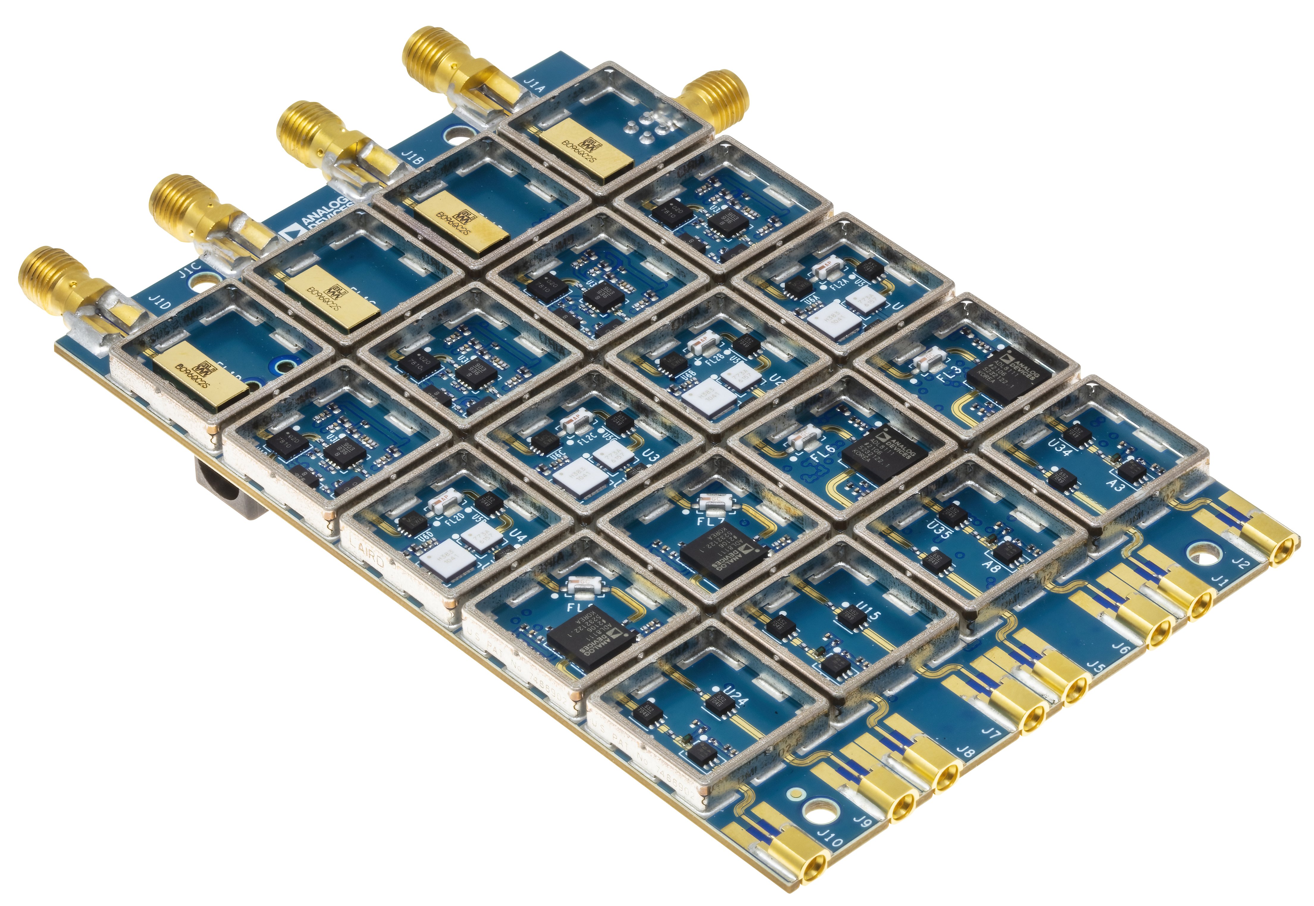
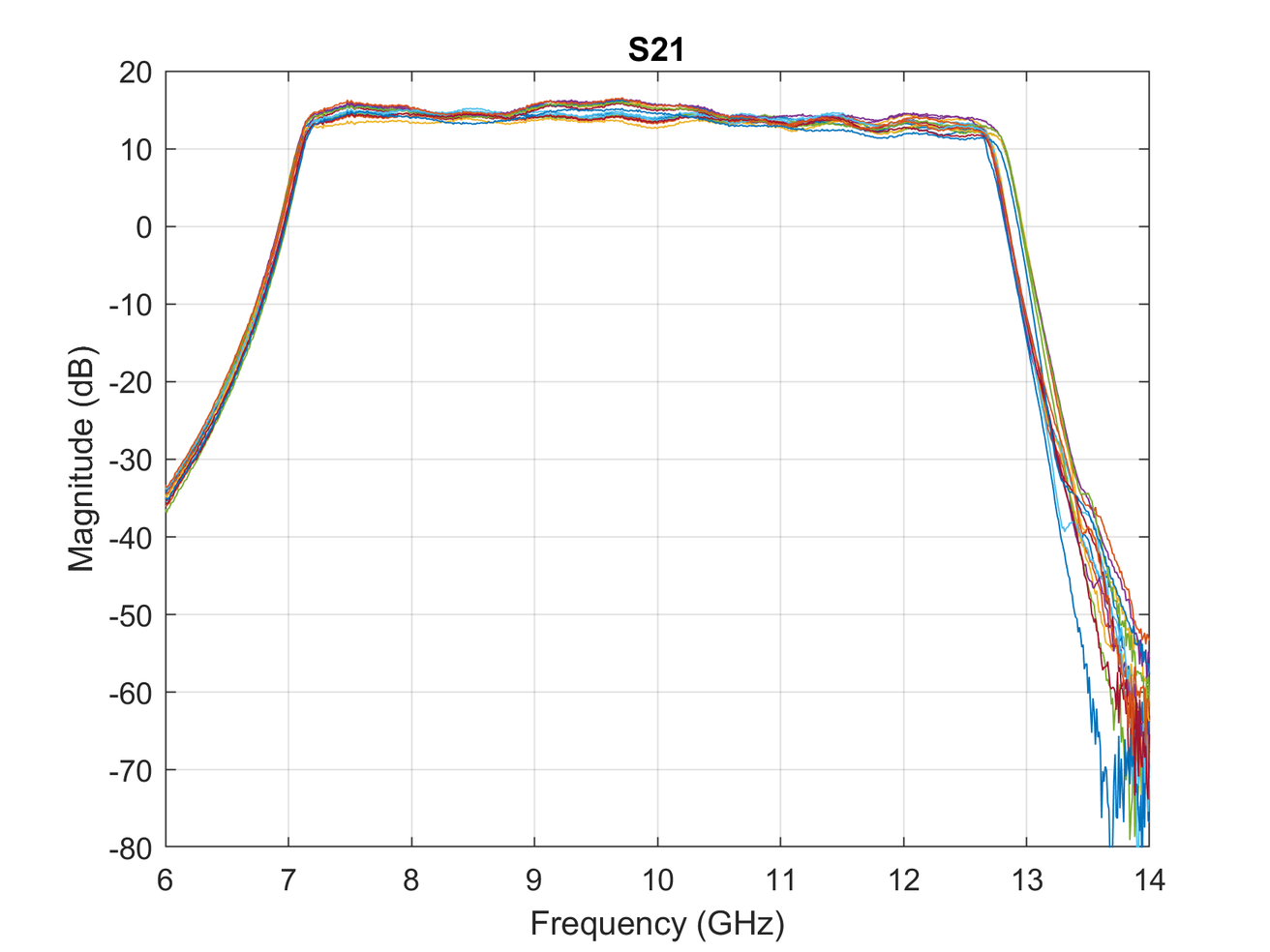
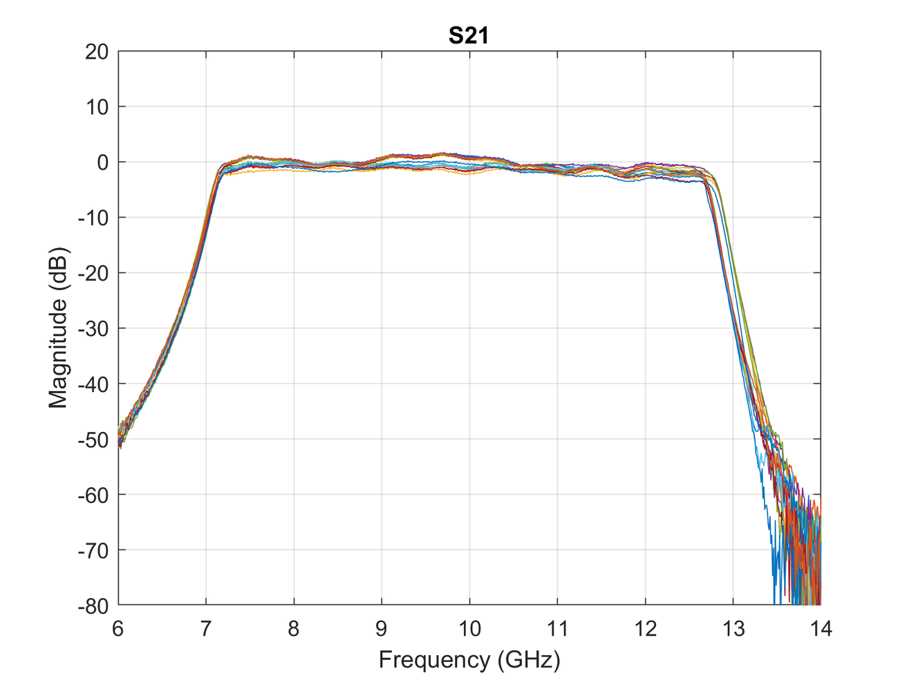
The ADXUD1AEBZ is a quad-channel X/C band frequency converter that bridges the gap between X-Band RF signals (8–12 GHz) used by the ADAR1000 beamforming board and the C-Band IF signals (4.2–6.3 GHz) that the AD9081 MxFE can process.
Overview
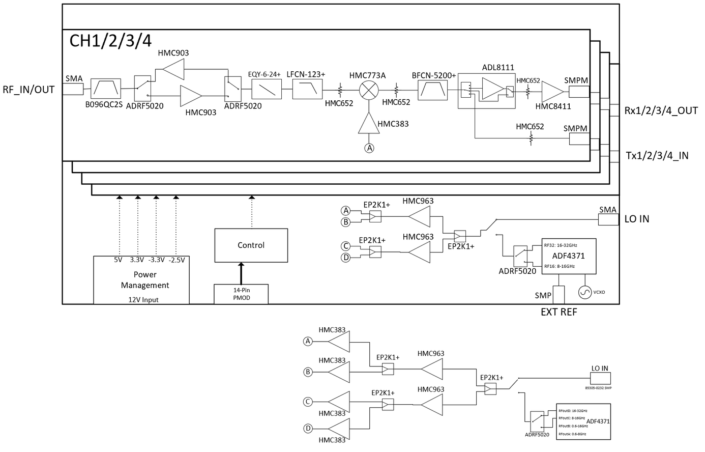
The ADXUD1AEBZ provides four independent up/down converter channels. Each channel contains a mixer (HMC773A), IF amplifiers (ADL8111, HMC8411), TX/RX amplifiers (HMC903), and an RF switch (ADRF5020) for TX/RX path selection. A common LO distribution network feeds all four channels from either an external source or the on-board ADF4371 PLL.
Tip
Schematics & Resources
Interposer Board
Component Product Pages
Block Diagram
Key Specifications
Parameter |
Value |
|---|---|
RF Frequency Range |
8 – 12 GHz |
IF Frequency Range |
4.2 – 6.3 GHz |
Number of Channels |
4 (independent TX/RX) |
RF Connectors |
4× SMA-F |
IF Connectors |
8× SMPM (4 TX + 4 RX) |
LO Input |
SMA-F (external) or on-board ADF4371 |
Supply Voltage |
12V DC |
Power Consumption |
~15W |
RF Performance
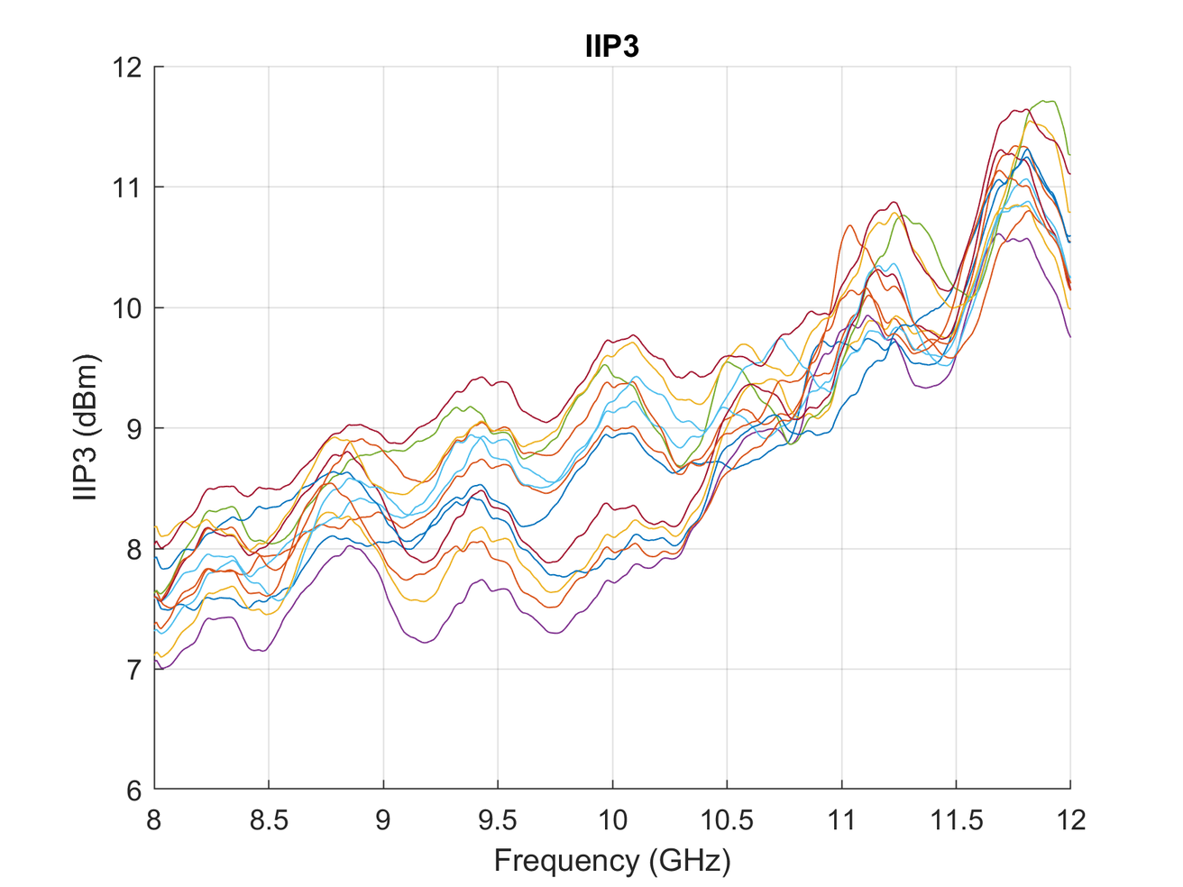
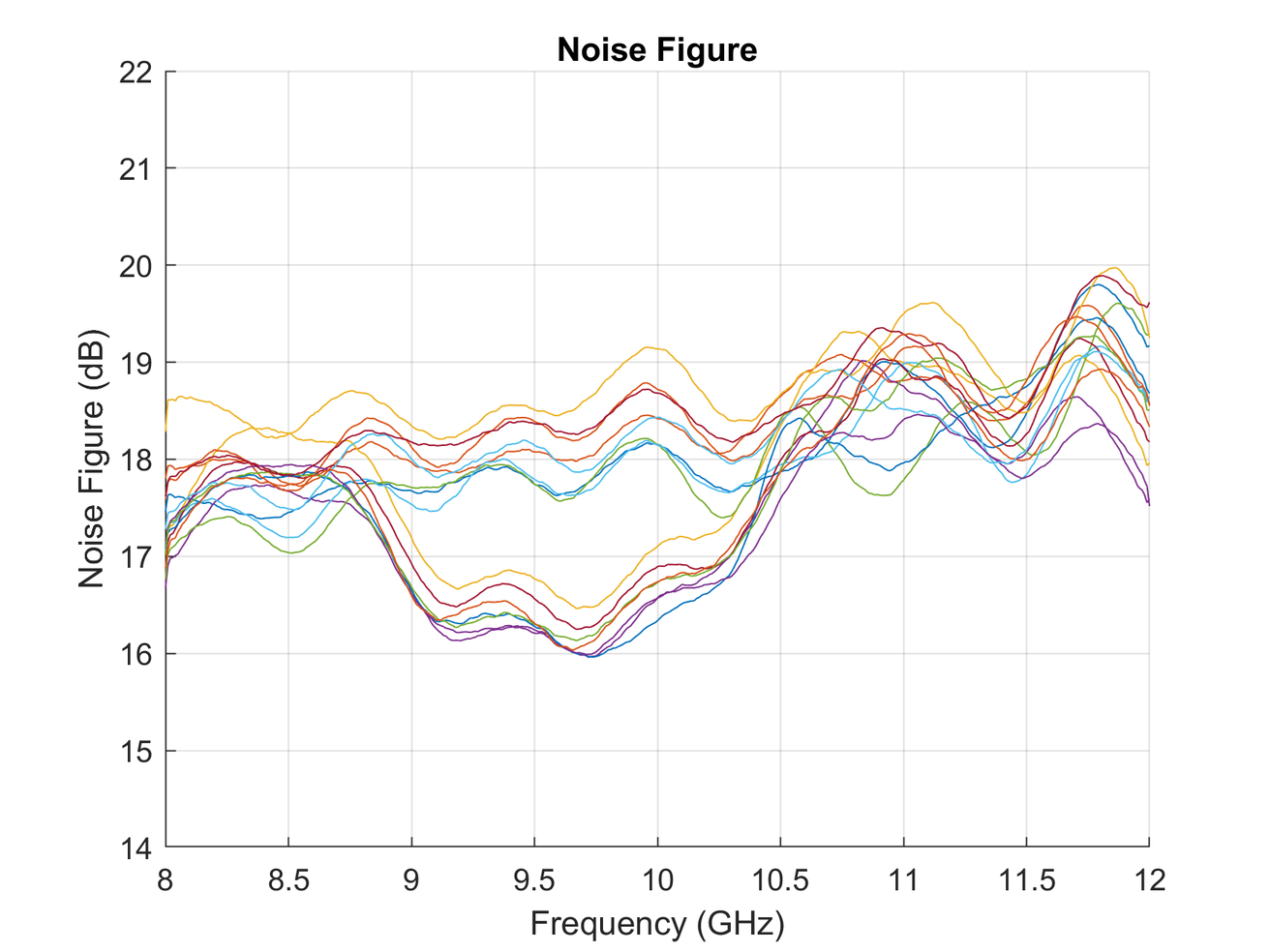
Receive — High Gain Mode
Frequency |
Gain (dB) |
Noise Figure (dB) |
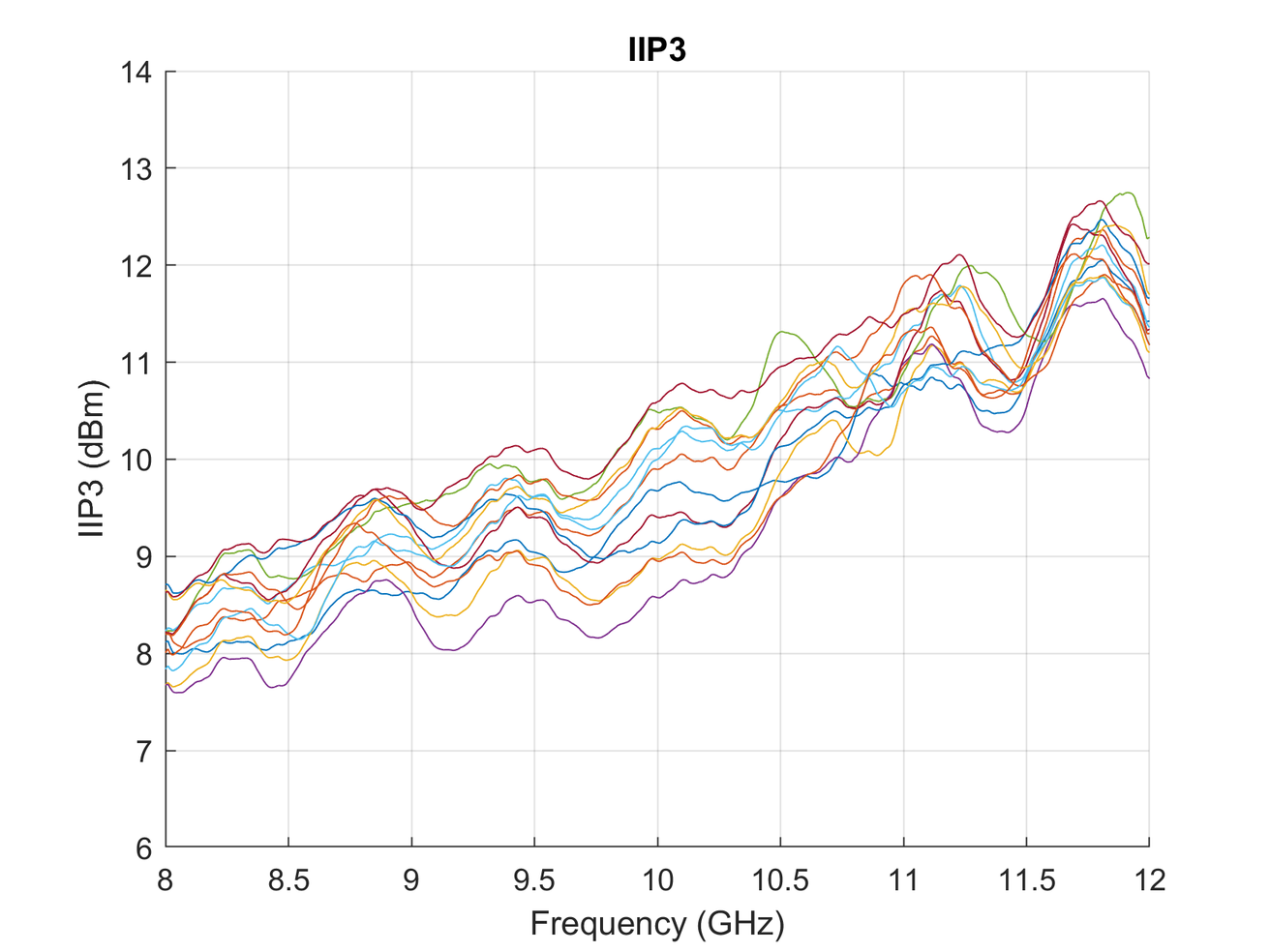
IIP3 (dBm) |
|---|---|---|---|
8 GHz |
14.63 |
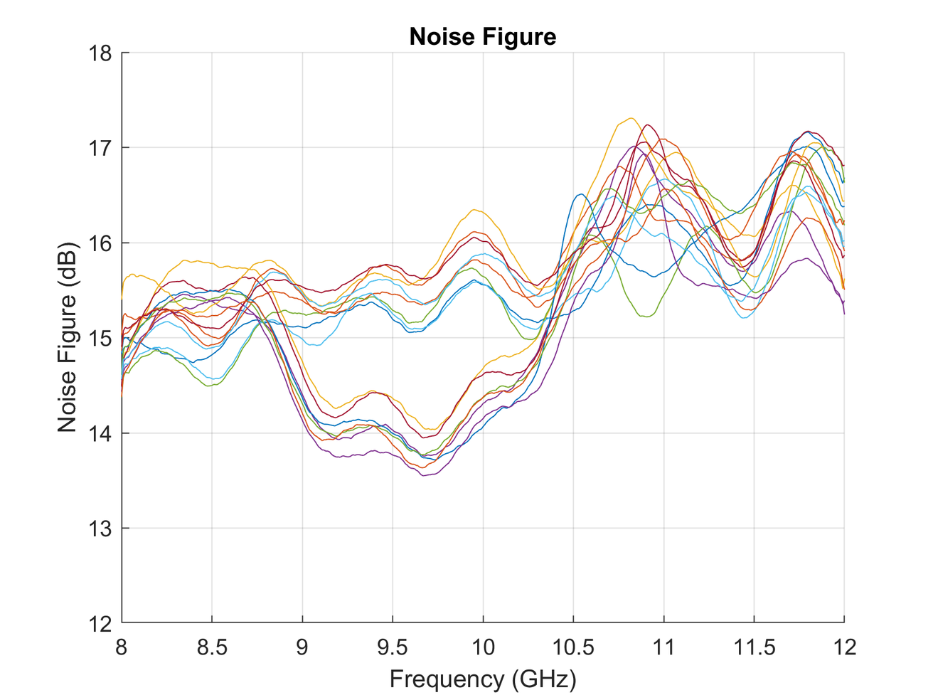
14.72 |
7.59 |
12 GHz |
13.38 |
16.17 |
10.40 |
Receive — Low Gain Mode
Approximately 14 dB lower gain than high-gain mode with improved linearity.
Transmit Mode
Parameter |
Value |
|---|---|
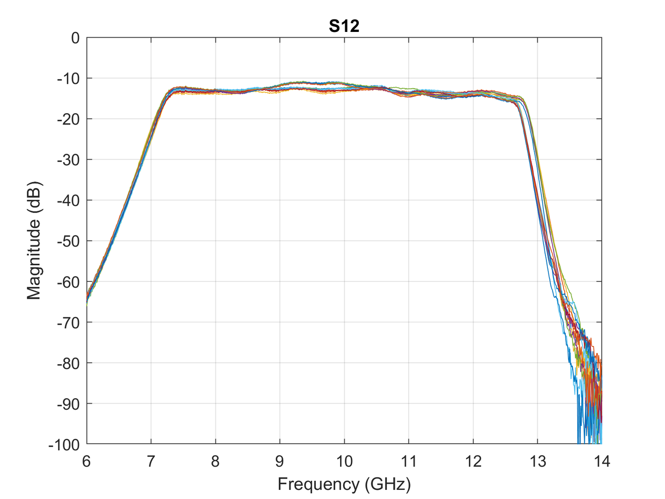
Conversion Gain |
−12 to −14 dB |
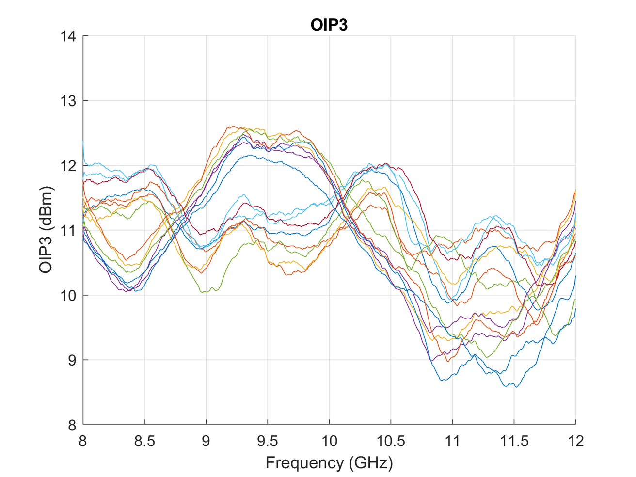
OIP3 |
Comparable to RX IIP3 |
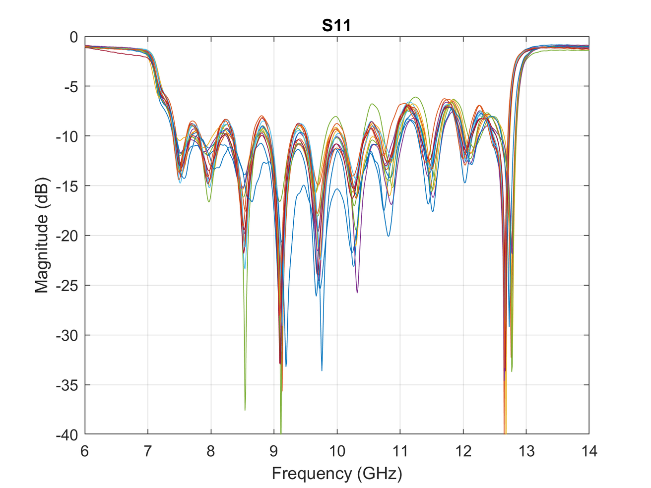
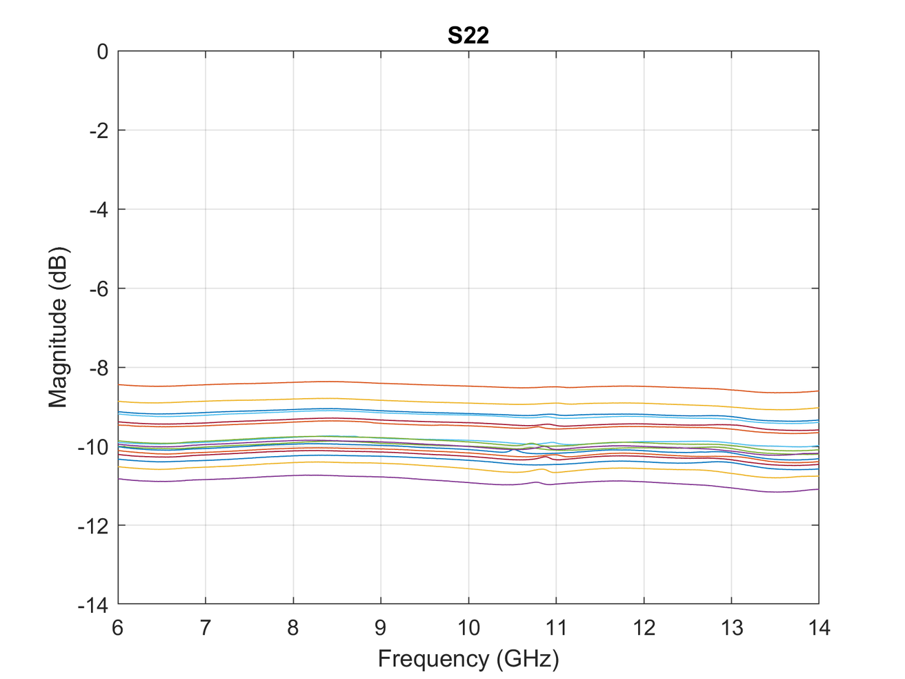
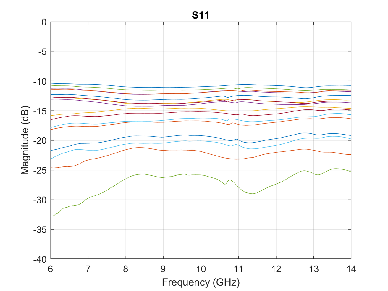
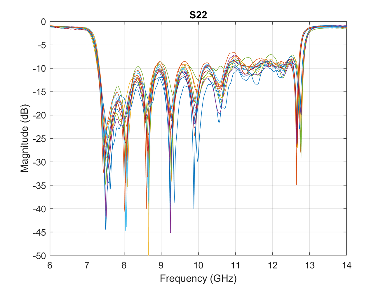
Return Loss
Board Architecture
Key Components
Component |
Function |
|---|---|
ADRF5020 |
RF TX/RX switch (4× per board) |
HMC773A |
Mixer — frequency conversion |
HMC903 |
TX/RX RF amplifier |
ADL8111 |
IF variable-gain amplifier |
HMC8411 |
IF amplifier |
ADF4371 |
On-board wideband PLL/VCO (optional LO) |
Connector Layout
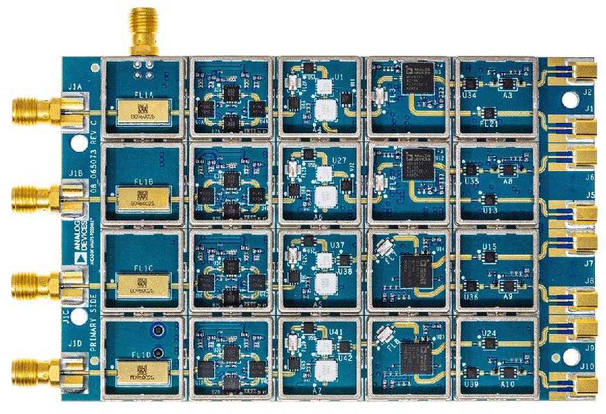
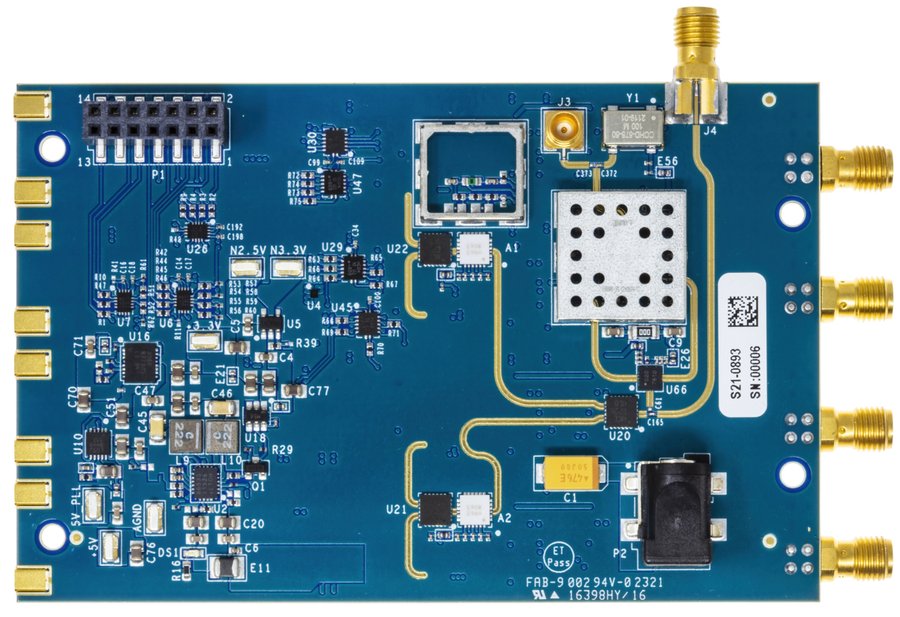
Control Interface
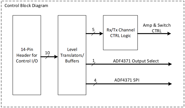
Digital control operates at 1.8V logic with on-board level translation to 3.3V. Two interface options are available:
PMOD Interface
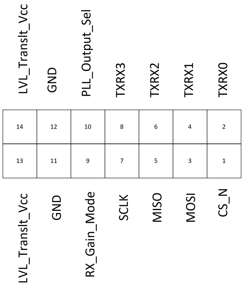
The PMOD connector enables GPIO and SPI communication for:
Per-channel TX/RX switching
Switchable receive gain (high/low)
SPI programming of the ADF4371 PLL
SDP-S Interface
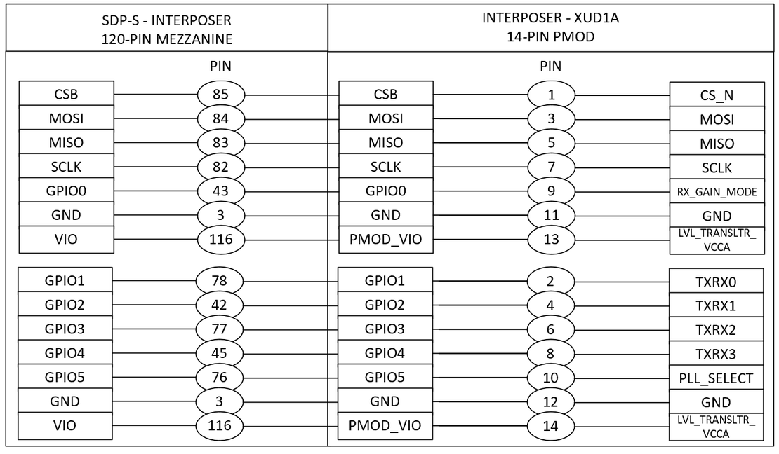
Alternative control path via the SDP-S connector for standalone evaluation without an FPGA.
Connection to ZCU102
ZCU102 HPC1 Connector → FMC extension cable → Interposer Board → PMOD cable → XUD1A
Optional: 14-pin 6-inch PMOD cable for easier RF access when shields are installed
LO Configuration
The ADXUD1AEBZ supports both external and internal LO sources:
External LO (default): Signal fed via SMA-F connector, distributed to all four channels through an on-board splitter network
On-board ADF4371 PLL: Generates LO internally using a 100 MHz on-board VCXO reference or an external reference clock
Refer to the Clocking Configuration page for details on switching between these options.
Switching Speed
Measured TX/RX switching performance:
Rising edge: ~159 ns average
Falling edge: ~14 ns average
Note
The on-board IF bandpass filters (FL3, FL6, FL7, FL8) provide basic filtering. Additional external filters (VLF-8400+, VLF-5500+) are recommended for optimized system performance to suppress mixing products, LO feedthrough, and DAC images.