CED1Z FPGA Project for AD7606 with Nios II
Supported Devices
Evaluation Boards
Overview
This document presents the steps to set up an environment for evaluating the EVAL-AD7606EDZ, EVAL-AD7606-6EDZ, or EVAL-AD7606-4EDZ evaluation board together with the EVAL-CED Converter Evaluation and Development (CED) Board and the Nios II Embedded Development Suite (EDS).
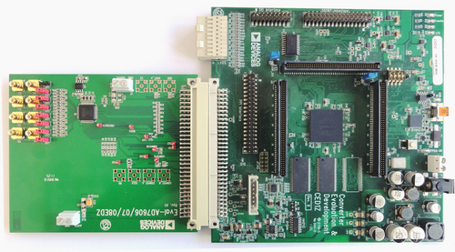
The CED1Z board is intended for use in evaluation, demonstration, and development of systems using Analog Devices precision converters. It provides the necessary communications between the converter and the PC: programming or controlling the device, transmitting or receiving data over a USB link.
The AD7606, AD7606-6, and AD7606-4 are 16-bit, 8/6/4 channel, simultaneous sampling Analog-to-Digital Data Acquisition systems (DAS). They contain analog input clamp protection, a second-order anti-alias filter (22 kHz, 3 dB cutoff), track-and-hold amplifier, 16-bit charge redistribution successive approximation ADC, flexible digital filter, 2.5 V reference and reference buffer, and high-speed serial and parallel interfaces.
These devices operate from a single 5 V supply and can accommodate ±10 V and ±5 V true bipolar input signals while sampling at throughput rates up to 200 kSPS for all channels. The input clamp protection circuitry can tolerate voltages up to ±16.5 V. The AD7606 has 1 MΩ analog input impedance regardless of sampling frequency. Single supply operation, on-chip filtering, and high input impedance eliminate the need for driver op-amps and external bipolar supplies.
The AD7606 anti-alias filter has a 3 dB cut-off frequency of 22 kHz and provides 40 dB anti-alias rejection when sampling at 200 kSPS. The flexible digital filter is pin-driven, yields improvements in SNR, and reduces the 3 dB bandwidth.
More Information
AD7605 Product Info — pricing, samples, datasheet
AD7605-4 Product Info — pricing, samples, datasheet
AD7606 Product Info — pricing, samples, datasheet
AD7606-6 Product Info — pricing, samples, datasheet
AD7606-4 Product Info — pricing, samples, datasheet
Getting Started
Hardware Items
The following hardware items are required:
Analog Devices EVAL-CED Converter Evaluation and Development (CED) Board
One of the following evaluation boards:
Intel Pentium III or compatible Windows PC running at 866 MHz or faster, with a minimum of 512 MB of system memory
Software Tools
The following software tools are required:
Quartus II Web Edition design software v11.0
Nios II EDS v11.0
The Quartus II design software and the Nios II EDS are available via the Altera Complete Design Suite DVD or by downloading from the web.
Install the USB-Blaster Device Driver
The Terasic USB-Blaster is used to program the CED1Z FPGA and connect to the Nios II JTAG debug port. Follow these steps to install the Windows device driver:
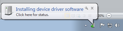
Plug the USB-Blaster into a free USB port on your PC. Windows will detect the new device.
Open Device Manager. The USB-Blaster will appear as an unrecognized device under “Other devices”.
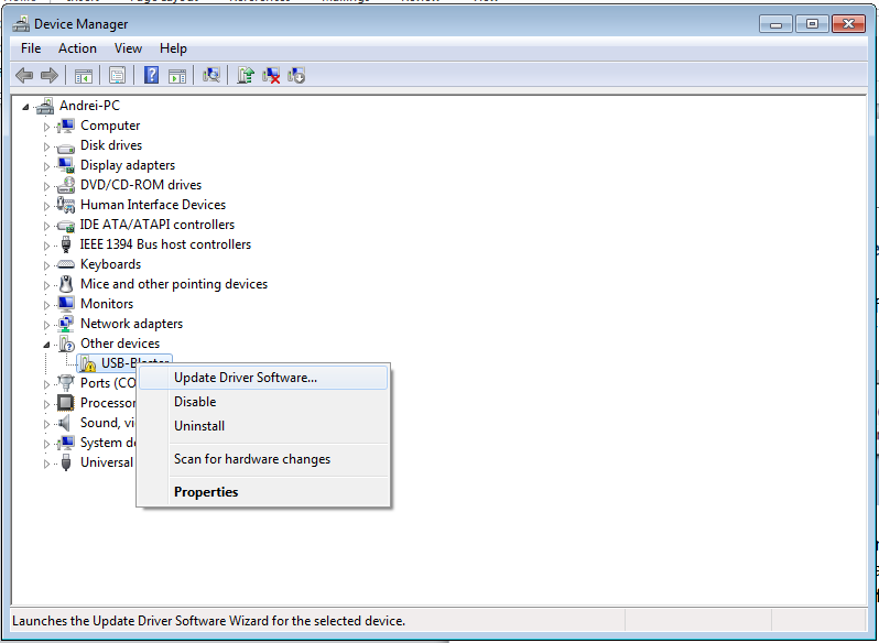
Right-click the device and select “Update Driver Software”. Choose “Browse my computer for driver software”.
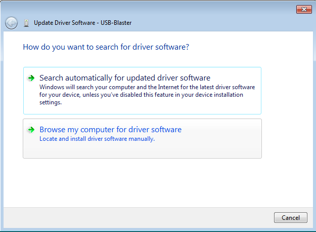
Browse to the Quartus II installation directory:
altera\11.0\quartus\drivers\usb-blaster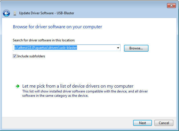
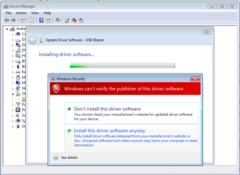
Click Next to proceed with the installation. Windows may warn about an unsigned driver — click “Install this driver software anyway”.
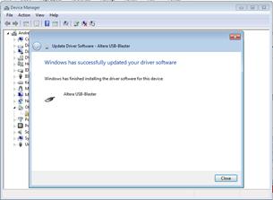
The USB-Blaster driver is now installed successfully.
AD7606 Evaluation Project Overview
The following sections describe the CED1Z FPGA design and the AD7606 peripheral interface implemented in the evaluation project.
CED1Z FPGA Design
The following components are implemented in the FPGA design:
Name |
Address |
IRQ |
|---|---|---|
CPU |
0x00000800 |
- |
PLL |
0x00000000 |
- |
ONCHIP_MEM |
0x00002000 |
- |
LEDS |
0x00000010 |
- |
SYSID |
0x00000020 |
- |
SRAM |
0x00200000 |
- |
TRISTATE_BRIDGE_0 |
- |
- |
JTAG_UART_0 |
0x00000030 |
1 |
SYS_TIMER |
0x00000040 |
2 |
MM_CONSOLE_MASTER |
- |
- |
PWR_DATA |
0x00000060 |
- |
I2C_INT |
0x00000080 |
- |
PWR_EN_CLK |
0x000000a0 |
- |
AD7606_0 |
0x000000c0 |
- |
The Nios II processor contains a peripheral that implements the communication protocol with the DUT. The peripheral is divided into three logical modules: a module which implements the interface with the Avalon bus and communication with the SRAM, a module which implements an Avalon master interface used to write data directly to the SRAM, and a module which communicates with the AD7606.
AD7606 Peripheral Port Definitions
Port |
Direction |
Width |
Description |
|---|---|---|---|
Generic pins |
|||
CLK_I |
IN |
1 |
System clock. Designed with a 98 MHz clock |
RESET_I |
IN |
1 |
System reset |
Avalon Slave Interface |
|||
AVALON_WRITEDATA_I |
IN |
32 |
Slave write data bus |
AVALON_WRITE_I |
IN |
1 |
Slave write data request |
AVALON_READ_I |
IN |
1 |
Slave read data request |
AVALON_ADDRESS_I |
IN |
3 |
Slave address bus |
AVALON_READDATA_O |
OUT |
32 |
Slave read data bus |
Avalon Master Interface |
|||
AVALON_MASTER_WAITREQUEST |
IN |
1 |
Master wait request signal |
AVALON_MASTER_ADDRESS_O |
OUT |
32 |
Master address bus |
AVALON_MASTER_WRITE_O |
OUT |
1 |
Master write signal |
AVALON_MASTER_BYTEENABLE_O |
OUT |
2 |
Master byte enable signals |
AVALON_MASTER_WRITEDATA_O |
OUT |
16 |
Master write data bus |
External connectors |
|||
ADC_DB_I |
IN |
16 |
ADC data bus used to read data from the AD7606 |
ADC_BUSY_I |
IN |
1 |
ADC Busy Output. Logic output that indicates conversion status. BUSY goes high after CONVST falling edge and stays high during conversion. Goes low when conversion is complete. |
ADC_OS_O |
OUT |
3 |
Oversampling Mode Pins used to select the oversampling ratio |
ADC_RANGE_O |
OUT |
1 |
Analog Input Range Selection. Logic high = ±10 V for all channels; logic low = ±5 V |
ADC_CS_N_O |
OUT |
1 |
ADC Chip Select. Active low input used with RD to read conversion data |
ADC_RD_N_O |
OUT |
1 |
ADC Read pin. Active low input used with CS to access conversion result |
ADC_RESET_O |
OUT |
1 |
Reset pin. Rising edge on RESET resets the AD7606 |
ADC_STDBY_O |
OUT |
1 |
Standby Mode pin. Used to place AD7606 into power-down modes |
ADC_CONVST_N_O |
OUT |
1 |
ADC Conversion Start Input. Falling edge on CONVST initiates conversion |
AD7606 Peripheral Registers
Name |
Offset |
Width |
Access |
Description |
|---|---|---|---|---|
CONTROL_REGISTER |
0 |
32 |
RW |
Bit 0: Start data acquisition; Bit 1: Initiate software reset; Bit 2: Configure Avalon write master to write to same location; Bit 3: Write data to EVAL-AD7606 evaluation board |
ACQ_COUNT_REGISTER |
1 |
32 |
RW |
Register to configure number of samples to acquire |
BASE_REGISTER |
2 |
32 |
RW |
Register to configure base memory address for acquired data |
STATUS |
3 |
32 |
R |
Bit 0: Acquisition complete; Bit 1: Internal memory buffer overflow; Bit 2: Write to read-only register |
DUT_WRITE_REGISTER |
4 |
32 |
W |
Register to configure driver submodule |
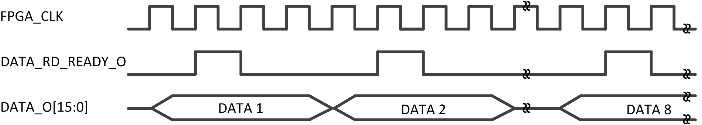
Nios II Read Timing Diagram
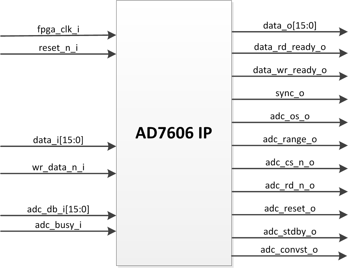
AD7606 Module
This module is the actual driver of the AD7606 data acquisition system.
Port |
Direction |
Width |
Description |
|---|---|---|---|
General Connectors |
|||
FPGA_CLK_I |
IN |
1 |
48 MHz clock |
ADC_CLK_I |
IN |
1 |
20 MHz clock |
RESET_I |
IN |
1 |
Module reset |
CED1Z Interface connectors |
|||
WR_DATA_N_I |
IN |
1 |
Signal to write data in driver’s internal registers |
DATA_I |
IN |
16 |
Data bus to configure driver |
DATA_O |
OUT |
16 |
Parallel bus to transfer data to upper module |
DATA_RD_READY_O |
OUT |
1 |
Signals new data available at DATA_O port |
DATA_WR_READY_O |
OUT |
1 |
Signals write from upper module has been performed |
SYNC_O |
OUT |
1 |
Signals next data transfer corresponds to channel 1 |
AD7606 connectors |
|||
ADC_DB_I |
IN |
16 |
ADC data bus to read data from AD7606 |
ADC_BUSY_I |
IN |
1 |
ADC Busy Output indicating conversion status |
ADC_OS_O |
OUT |
3 |
Oversampling Mode Pins to select oversampling ratio |
ADC_RANGE_O |
OUT |
1 |
Analog Input Range Selection (high = ±10 V, low = ±5 V) |
ADC_CS_N_O |
OUT |
1 |
ADC Chip Select (active low) |
ADC_RD_N_O |
OUT |
1 |
ADC Read pin (active low) |
ADC_RESET_O |
OUT |
1 |
Reset pin (active high) |
ADC_STDBY_O |
OUT |
1 |
Standby Mode pin |
ADC_CONVST_N_O |
OUT |
1 |
ADC Conversion Start Input (active low) |