Time Division Duplexing (TDD)
The X-Band platform implements Time Division Duplexing (TDD) through a TDD IP Core (axi-core-tdd) that provides hardware integration and firmware control for precise transmit/receive switching in radar applications.
TDD Components:
Hardware Layer: Interposer board with GPIO signal routing and distribution
Firmware Layer: TDD core implemented in ZCU102 FPGA programmable logic
Software Layer: Linux IIO drivers and Python API for configuration
Signal Layer: 6 synchronized control channels distributed to all boards
Key Features:
6-channel programmable frame-based timing structure
Precise control of TX/RX windows with microsecond resolution
Simultaneous coordination of AD9081, ADXUD1AEBZ, and ADAR1000 boards
Flexible sync triggering (soft command or external GPIO)
Flexible configuration for various radar modes (pulse, FMCW, etc.)
System Architecture
Hardware Components
The TDD Functional Package integrates the following hardware elements:
ZCU102 Zynq UltraScale+ MPSoC
Contains TDD core in programmable logic
Generates 6 GPIO control signals (TDD_CH0 to TDD_CH5)
Outputs signals via PMOD connector J55 on the Interposer
Runs embedded Linux with IIO framework for TDD configuration
Provides real-time timing control with FPGA precision
Interposer Board
Central hub for TDD signal distribution
Routes signals from ZCU102 to multiple destination boards
Provides signal buffering and level conversion as needed
Includes labeled signal lines: IMU_GPIO0, IMU_GPIO1, IMU_GPIO2
AD9081 MxFE (Mixed-Signal Front End)
Receives TX_EN and RX_EN control signals from TDD package
Controls transmit and receive data path enables
Synchronizes with JESD204B high-speed data interface
Provides DAC output during TX and ADC input during RX
ADXUD1AEBZ Up/Down Converter
Receives TR switch control signal
Switches between transmit and receive IF paths
Provides frequency conversion (X-band ↔ IF)
Maintains high TX/RX isolation during switching
ADAR1000 Beamformer Array
Receives TR switch control signal
Controls RF path switching via integrated T/R switches
Manages PA (Power Amplifier) and LNA (Low Noise Amplifier) bias
Provides fast switching times (sub-microsecond)
GPIO Signal Connections
TDD Channel Summary
The TDD core exposes 6 channels, each mapped to a specific hardware signal:
Channel |
Signal Name |
Function |
Destination |
|---|---|---|---|
CHAN[0] |
|
TX sync trigger |
AD9081 TX offload |
CHAN[1] |
|
RX capture window |
AD9081 RX offload |
CHAN[2] |
|
Master GPO enable |
All boards |
CHAN[3] |
|
MxFE RX path enable |
AD9081 RX path |
CHAN[4] |
|
MxFE TX path + XUD1A sync |
AD9081 TX path + Interposer Pin 13 |
CHAN[5] |
|
Stingray TX/RX switching |
ADAR1000 TR pin |
ZCU102 GPIO Mapping
Signal Descriptions
CHAN[0] — TX_OFFLOAD_SYNC
Function: Sync start trigger for the TX offload engine
Trigger Modes: Soft sync command (software-initiated) or external GPIO trigger
Destination: AD9081 TX offload (
TDD.CHAN[0])
CHAN[1] — RX_OFFLOAD_SYNC
Function: Defines the RX data capture window
Parameters: Controlled by
on_ms(start),off_ms(end), startup delay, and RX buffer sizeStartup Delay: Configurable delay from sync trigger before the RX window opens
Destination: AD9081 RX offload (
TDD.CHAN[1])
CHAN[2] — TDD_ENABLE
Function: Master GPO enable bit for the TDD engine
Behavior: When set, TDD waveform generation and control logic become active. Must share timing with
TX_MXFE_EN(CHAN[4]) andTX_STINGRAY_ENABLE(CHAN[5])Important: Keep this high during all TDD operation. When configuring TDD properties, set high and leave high
Default State: Starts low — no data can be received until this is enabled
CHAN[3] — RX_MXFE_EN
Function: Intended to enable the RX path of the MxFE during the receive window defined by the TDD schedule
Current Status: Not actively used based on testing — does not produce functional output in current firmware
CHAN[4] — TX_MXFE_EN
Function: GPIO that controls the TX/RX state of the XUD1A up/down converter board. High = TX enabled, Low = RX enabled
Dual Role: Also controls XUD1A sync timing through Pin 13 of the Interposer board
Behavior: When high, the TX buffer plays out. When it goes low, any remaining TX buffer content is truncated
use_tx_mxfe_enflag:use_tx_mxfe_en = 0: CHAN[4] stays high for the fullframe_length_msdurationuse_tx_mxfe_en = 1: CHAN[4] pulses high only fortx_time, then returns low — enabling multiple TX bursts per frame
CHAN[5] — TX_STINGRAY_ENABLE
Function: GPO output to the Stingray board that enables the TX path on the ADAR1000
Behavior: When low and polarity = 0, RX is enabled on the Stingray
Timing: Should match CHAN[4] timing (same timing as TX_MXFE_EN for synchronized TX/RX switching)
Note: This channel can also be repurposed as a general programmable GPO
Physical Connections
FPGA Pin → FMC → Interposer Mapping
Signal |
FPGA Pin |
FMC Connector |
Interposer Pin |
|---|---|---|---|
MxFE TX EN |
AG3 |
D11 |
P3-13 |
MxFE RX EN |
AH3 |
D12 |
P3-14 |
External Sync |
AE2 |
D14 |
P3-15 |
ZCU102 PMOD J55 Connector
Type: 2×6 pin header (12 pins total, 0.1” pitch)
Location: On ZCU102 carrier board
Signals Used: Pins 13, 14, 15 (CHAN[0]–[2]), Pin 7 (Ground)
Voltage Levels: 3.3V CMOS compatible
Cable: Connects to interposer board via ribbon cable
Interposer Board Distribution
Input: Receives signals from ZCU102 PMOD J55
Buffering: Provides signal conditioning and drive capability
Output Routes:
IMU_GPIO0 → AD9081 TX offload sync (CHAN[0])
IMU_GPIO1 → AD9081 RX offload sync (CHAN[1])
IMU_GPIO2 → Master TDD enable (CHAN[2])
Pin 13 → XUD1A sync (driven by CHAN[4])
Common Ground: Maintains consistent reference across all boards
RX Buffer Operation
Continuous Listening
An important characteristic of the X-Band system is that the RX buffer (ADC) is always listening and continuously sampling the RF environment:
Always Active: The ADC hardware continuously converts received RF signals to digital samples
No Timing Required: The receiver does not need to be timed to “catch” returning TX echoes as the TX and RX buffers begin in sync.
Continuous Sampling: ADC samples are generated continuously, regardless of TDD state
Data Capture Window: The RX_EN signal (TDD_CH1) only controls which samples are captured and processed
RX_EN Function Clarification
The RX_EN signal does NOT control when the hardware listens. Instead, it controls:
Data Capture Gating: Which ADC samples are saved/buffered for processing
JESD204B Streaming: When data is actively streamed to the processor
Processing Window: Which samples are passed to signal processing algorithms
Memory Management: Prevents buffer overflow by limiting captured data
Practical Implications
For Pulsed Radar (Continuous TX, Buffered Capture):
TDD generates TX pulses infinitely (frames repeat continuously)
ADC continuously runs and samples all frames
RX buffer size determines how many pulses are captured
Example: Frame length = 1 ms, buffer size = 100 ms → captures 100 TX pulses
After buffer fills, processing analyzes the captured pulses for coherent integration
RX_EN can be HIGH continuously to capture all data, or windowed per frame
For FMCW Radar:
TDD frames repeat continuously (continuous chirping)
ADC continuously samples the mixed TX/RX signal
RX_EN typically stays HIGH continuously
Frame length typically matches chirp duration
Buffer size determines how many chirps are captured for processing
Buffer Size and Frame Relationship:
TDD frames transmit infinitely once enabled
RX buffer acts as a “snapshot” capturing N frames worth of data
Number of pulses captured = (Buffer Size) / (Frame Length)
Once buffer is full, data is processed and buffer can be restarted
This allows continuous radar operation with periodic signal processing
Advantages:
Simplifies timing constraints
Reduces risk of missing target returns due to timing errors
Allows flexibility in defining capture windows
TDD Frame Structure
Frame-Based Operation
The TDD core operates using a frame-based timing model. Each frame represents one TX cycle (pulse) and repeats infinitely.
How TDD and RX Buffer Interact:
TDD Operation: Once enabled, TDD frames repeat continuously, generating TX pulses indefinitely
RX Buffer Capture: The RX buffer size is set to be a multiple of the frame length
Pulse Count: Number of captured pulses = (RX Buffer Size) / (Frame Length)
Example: If frame length = 1 ms and RX buffer = 100 ms, you capture 100 TX pulses
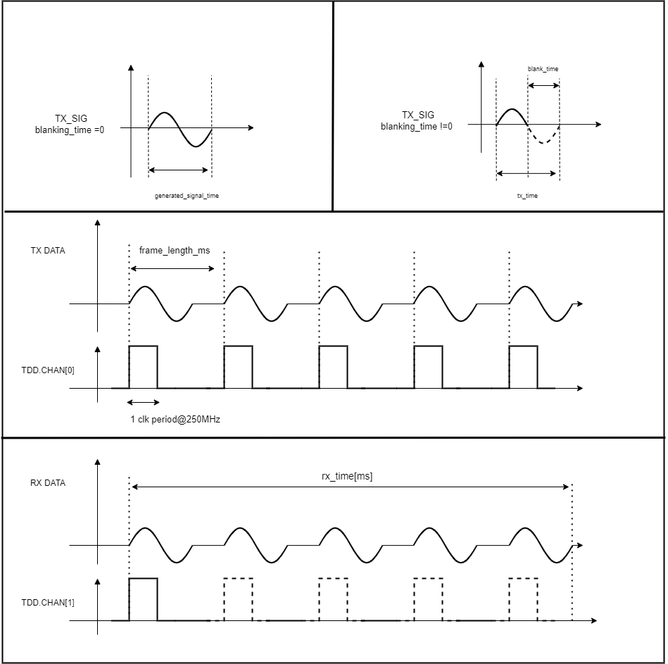
Understanding the Frame Structure Diagram
The diagram above illustrates the key concepts of TDD frame-based operation.
Operation:
Continuous Operation: Once TDD is enabled, frames repeat indefinitely (Frame 1, Frame 2, Frame 3… Frame N)
Each Frame Identical: Every frame has the same structure with one TX pulse and one RX capture window
Buffer Determines Capture: The RX buffer spans multiple frames, capturing data from N consecutive frames
Pulse Count: The number of TX pulses captured equals Buffer Size ÷ Frame Length
Note
Key Insight: The TDD system repeats frames continuously once TDD_ENABLE (CHAN[2]) is asserted. You control how many pulses are captured by setting the RX buffer size. If your frame is 1 ms, TX pulse is 0.5 ms, and you want 100 pulses, set your RX buffer to 100 ms.
Timing Parameters
The TDD frame structure is defined by programmable timing parameters:
Frame Length
Definition: Total duration of one complete TDD cycle
Typical Range: 1 µs to several milliseconds
Units: Can be specified in time units or clock cycles
Considerations: Must accommodate TX pulse, guard times, and RX window
Channel ON/OFF Times
Definition: Start and stop times for each TDD channel within the frame
Resolution: Sub-microsecond precision
Configuration: Each channel (CH0, CH1, CH2) independently programmable
Reference: All times relative to frame start (t=0)
RX Buffer Size
TDD Behavior: TDD frames repeat infinitely once enabled (continuous TX pulsing)
Capture Control: The RX buffer size determines how many pulses are captured
Calculation: Number of Captured Pulses = (RX Buffer Size) / (Frame Length)
Example: Frame length = 1 ms, RX buffer = 128 ms → captures 128 TX pulses
Secondary Times
Definition: Optional additional ON periods within the same frame
Usage: Enables multi-pulse modes or complex waveform generation
Configuration: Secondary ON/OFF times can be set for each channel
Example Timing Configuration
For a simple pulsed radar with 10 µs TX pulse per frame:
Frame Length: 20 µs

TDD_CH0 (TX Enable):
  - ON time:  0 µs
  - OFF time: 10 µs
  - Duration: 10 µs TX pulse (repeats every frame)

TDD_CH1 (RX Enable):
  - ON time:  0 µs
  - OFF time: 20 µs
  - Duration: 20 µs capture window per frame

TDD_CH2 (TR Switch):
  - ON time:  0 µs (TX mode)
  - OFF time: 10 µs
  - Switches to RX ahead of data enables

RX Buffer Size: 100 µs
Result: TDD pulses for 10 µs every 20 µs period
        RX buffer captures 5 TX pulses (100 µs / 20 µs per frame)
        After buffer fills, you have 5 pulses for coherent processing
TDD Configuration Methods
Software Interface
The TDD core is controlled through the Linux IIO (Industrial I/O) framework:
IIO Device
Device Name:
axi-core-tddType: IIO trigger device
Driver: Analog Devices TDD core driver
Location:
/sys/bus/iio/devices/iio:deviceX/
Configuration Attributes
Frame Length: Sets total frame duration
Channel ON/OFF Times: Configures timing for each of the 3 channels
Enable: Starts/stops TDD operation
Secondary Timing: Optional additional pulse periods
ADAR1000 Beamformer Switching
TR Switch Control (CHAN[5] → TX_STINGRAY_ENABLE → TR Pin)
Function: Controls integrated T/R switches in each ADAR1000
TX Mode (HIGH):
RF switches route signal to PA (Power Amplifier) path
PA bias enabled for transmit amplification
LNA (Low Noise Amplifier) disabled/protected
RX Mode (LOW, polarity=0):
RF switches route signal to LNA path
LNA bias enabled for low-noise amplification
PA disabled to save power and reduce noise
Switching Time: Sub-microsecond transition
Isolation: High TX/RX isolation protects receiver
ADXUD1AEBZ Up/Down Converter Switching
TX/RX Control (CHAN[4] → TX_MXFE_EN → Interposer Pin 13)
Function: Switches IF signal paths between TX and RX on the XUD1A
TX Mode (HIGH):
IF input from MxFE DAC routed to upconverter
Upconverter generates X-band TX signal
RX path disabled/isolated
RX Mode (LOW):
X-band RX signal routed to downconverter
Downconverter generates IF output to MxFE ADC
TX path disabled/isolated
Isolation: Maintains high TX/RX isolation for dynamic range
Monitoring and Verification
Signal Probe Points
Two key TDD signals are accessible for oscilloscope verification:
Signal |
Board |
Probe Location |
|---|---|---|
|
Interposer |
P3-13 |
|
Stingray |
TR pin |
Oscilloscope Verification
Recommended Measurements
TX_MXFE_EN: Probe P3-13 on the Interposer to verify XUD1A TX/RX switching timing
TX_STINGRAY_ENABLE: Probe the TR pin on the Stingray to verify ADAR1000 TX/RX switching
Guard Times: Measure actual delays between transitions
Frame Period: Verify frame repetition rate
Rise/Fall Times: Check signal quality and edge rates
Performance Considerations
Timing Resolution and Accuracy
Clock-Based Timing
Reference: All TDD timing derived from FPGA system clock
Typical Clock: 250 MHz system clock
Resolution: 4 ns per clock cycle
Accuracy: Depends on clock stability and jitter
Drift: Minimal drift with quality clock source
Configuration Units
Time Units: Microseconds (µs) or milliseconds (ms) for user interface
Internal Units: Clock cycles for FPGA implementation
Precision: Sub-microsecond precision available
Switching Performance
System Settling Times
RF Switches: ADAR1000 switches in < 1 µs
IF Switches: ADXUD1A converter switching < 2 µs
Amplifier Bias: PA/LNA bias settling 5-20 µs
Total TX→RX: Recommend 20-50 µs guard time minimum
Total RX→TX: Recommend 10-30 µs guard time minimum
Isolation Performance
TX/RX Isolation: Critical for receiver dynamic range
Switch Isolation: ADAR1000 provides >40 dB typical
Converter Isolation: ADXUD1A provides >35 dB typical
System Isolation: Combined isolation typically >30 dB
Leakage Impact: Insufficient isolation degrades sensitivity
Radar Performance Implications
Minimum Range
Limitation: TX-to-RX guard time sets minimum detectable range
Calculation: Min Range = (Guard Time × Speed of Light) / 2
Example: 30 µs guard time → ~4.5 km minimum range
Mitigation: Reduce guard time if system allows faster settling
Maximum PRF (Pulse Repetition Frequency)
Limitation: Frame length sets maximum PRF
Calculation: Max PRF = 1 / Frame Length
Example: 1 ms frame → 1 kHz PRF
Consideration: Must include TX pulse + guard + RX window + margin
Duty Cycle
Definition: Fraction of time spent transmitting
Calculation: Duty Cycle = TX Duration / Frame Length
Example: 100 µs TX / 1 ms frame = 10% duty cycle
Impact: Affects average transmit power and thermal management
Range-Doppler Ambiguity
Unambiguous Range: c / (2 × PRF)
Unambiguous Velocity: λ / (4 × Frame Length)
Trade-off: Frame length affects both range and velocity ambiguity
Resolution: Choice depends on application requirements