ADS7-V2EBZ High Speed Evaluation Board
Preface
The ADS7-V2EBZ was developed to support the evaluation of Analog Devices high speed A/D converters, D/A converters and transceivers with JESD204B bit rates up to 12.5 Gbps. The platform supports specified Analog Devices evaluation boards only. The ADS7-V2 is not intended to be used as a development platform, and no support is available for standalone operation.
For DAC-specific support documentation, refer to the ADS7 DAC evaluation guide.
Features
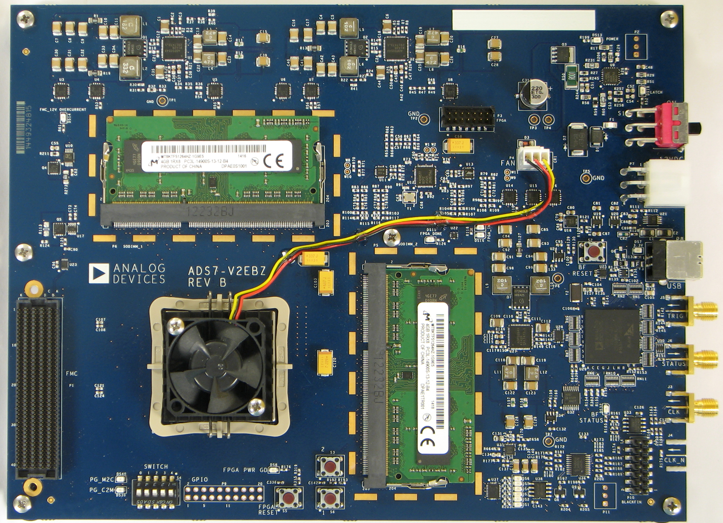
Xilinx Virtex-7 XC7VX330T-3FFG1157E FPGA (326,400 logic cells)
One FMC-HPC connector
Ten 13.1 Gbps transceivers via FMC-HPC
Two DDR3-1866 DIMMs
USB 2.0 interface
Using ADS7-V2EBZ for High Speed ADC Evaluation
Overview
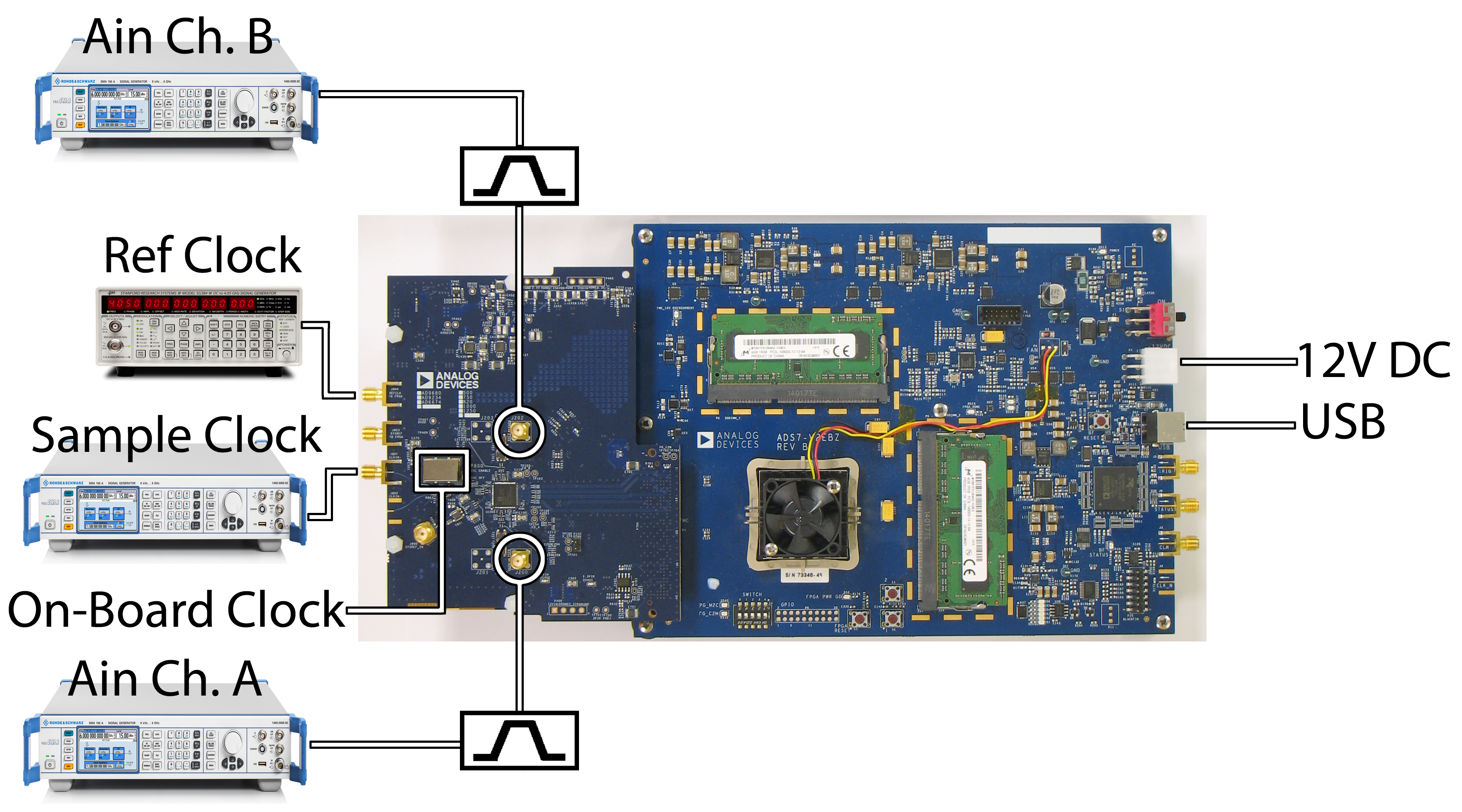
When used with the specified ADC evaluation boards, the ADS7-V2EBZ platform functions as a high speed data acquisition system. The FPGA on the ADS7-V2 acts as the data receiver, while the ADC is the data transmitter.
Helpful Documents
AN-905 Application Note, VisualAnalog Converter Evaluation Tool Version 1.0 User Manual
AN-878 Application Note, High Speed ADC SPI Control Software
AN-877 Application Note, Interfacing to High Speed ADCs via SPI
AN-835 Application Note, Understanding ADC Testing and Evaluation
Software Needed
Design Files
Complete schematic, BOM, Gerber files, and Cadence board design files are available in the ADS7-V2EBZ design files archive.
Supported ADC Boards
For a complete list of supported ADC evaluation boards, refer to the High Speed ADC Evaluation Boards product page.