Evaluating the AD9434 analog-to-digital converter using SDP-H1
Warning
Support for the ad9434fmc is not part of 2022_r2 Kuiper Linux release. Last release in which pre-build files can be found is 2021_r2. Check Kuiper Versions to see all Kuiper releases. All the sources remained in main branches, and probably it will be added back in next releases, being supported on Zed Board.
Preface
This user guide describes the evaluation board, AD9434-FMC-500EBZ, that is used to evaluate the following Analog Devices, Inc., product: AD9434. This evaluation board provide all the support circuitry required to operate these parts in their various modes and configurations. The application software used to interface with the devices is also described.
The AD9434 data sheet provide additional information and should be consulted when using the evaluation board. All documents and software tools are available at www.analog.com/sdp. For additional information or questions, send an email to highspeedproductssupport@analog.com.
Typical Measurement Setup
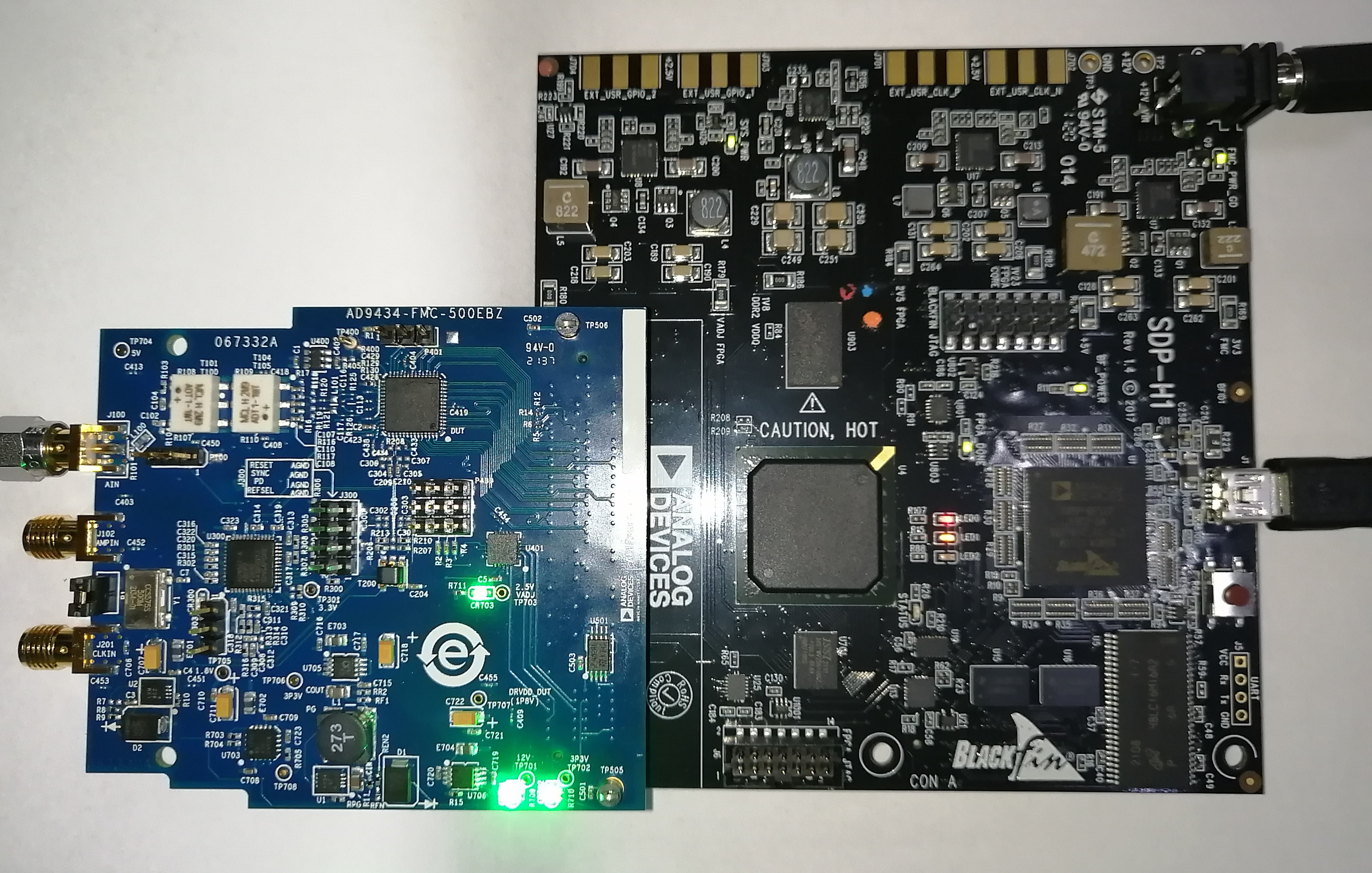
Figure 1 Evaluation Board Connection— AD9434-FMC-500EBZ (on Left) and EVAL-SDP-CH1Z SDP-H1 (on Right)
Features
Helpful Documents
AD9434 data sheet
EVAL-SDP-CH1Z, SDP-H1 High Speed Controller Board for System Development Platform
AN-905 Application Note, VisualAnalog Converter Evaluation Tool Version 1.0 User Manual
AN-878 Application Note, High Speed ADC SPI Control Software
AN-877 Application Note, Interfacing to High Speed ADCs via SPI
AN-835 Application Note, Understanding ADC Testing and Evaluation
UG-290 User Guide, User Guide for FIFO5 AD9434 Evaluation Board
Software Needed
Equipment Needed
Analog signal source (preferably SMA 100A Signal Generator)
Antialiasing filter
Sample clock source (if not using the on-board oscillator)
12V Power Supply
1-meter SMA Cable
PC running Windows®
USB-Mini-B Cable
AD9434-FMC-500EBZ board
EVAL-SDP-CH1Z System Development Platform Kit
Getting Started
This section provides quick start procedures for using the AD9434-FMC-500EBZ board. Both the default and optional settings are described.
Configuring the Board
Before using the software for testing, configure the evaluation board as follows:
Connect the evaluation board to the data capture board, as shown in Figure 1.
Connect one 12V switching power supply to the EVAL-SDP-CH1Z SDP-H1 board.
Connect the EVAL-SDP-CH1Z SDP-H1 board to the PC with a USB cable. (Connect to J1)
On using the on-board clock in the board, connect the Pin 1 and Pin 2 in P1.
On the ADC evaluation board, use a clean signal generator with low phase noise to provide an input signal to the input channel (J100). Use a 1 m, shielded, RG-58, 50 Ω coaxial cable to connect the signal generator: For best results, use a narrow-band, band-pass filter with 50 Ω terminations and an appropriate center frequency. (Analog Devices uses TTE, Allen Avionics, and K & L band-pass filters)
If using external clock signal, remove the connector in P1 and use a clean signal generator to J201.
Using The Software for Testing
Setting up the ADC Data Capture
After configuring the board, set up the ADC data capture using the following steps:
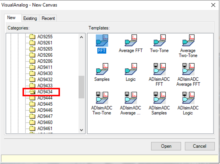
Start Visual Analog.

Select AD9434 and double click FFT
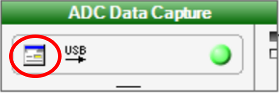
Click settings under ADC Data Capture.
Set device to Default.
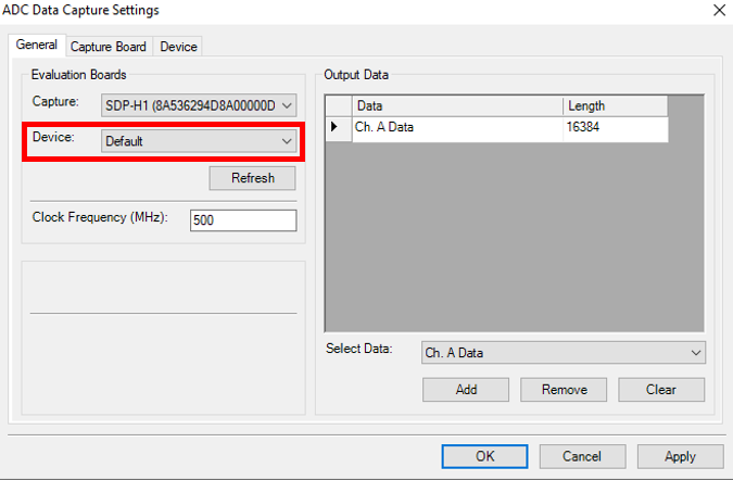
Navigate to Capture Board and browse your file directory for the FPGA Image called. (ad9434_sdph1.bin)
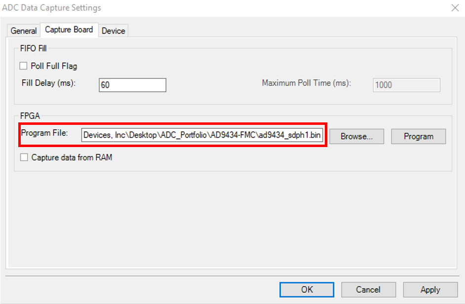
Click Program and check if LED0 on the SDP-H1 lights up. Then, click OK.
Evaluation And Test
Setting up the SPI Controller Software
Start SPIController

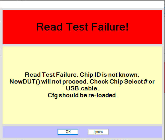
If a message opens saying “Read Test Failure”, select Ignore.
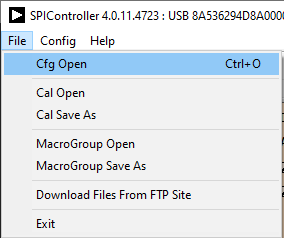
Click File > Cfg Open then find the file named “ad9434_12bit_500MSspiR03.cfg” and double click it.
Again, if a message opens saying “Read Test Failure”, select Ignore.
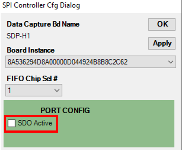
Click Config > Controller Dialog.
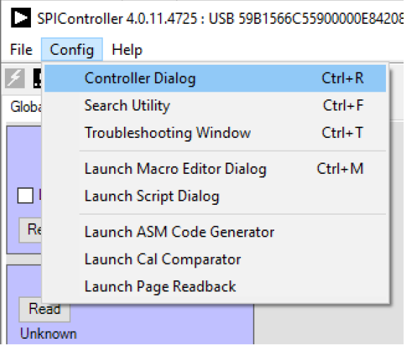
Unselect SDO Active and click OK
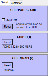
Click Read chip ID and Read Chip Grade.
Go Back to Visual Analog and click Play button.
Adjusting the Amplitude of the Input Signal
The next step is to adjust the amplitude of the input signal for each channel as follows:
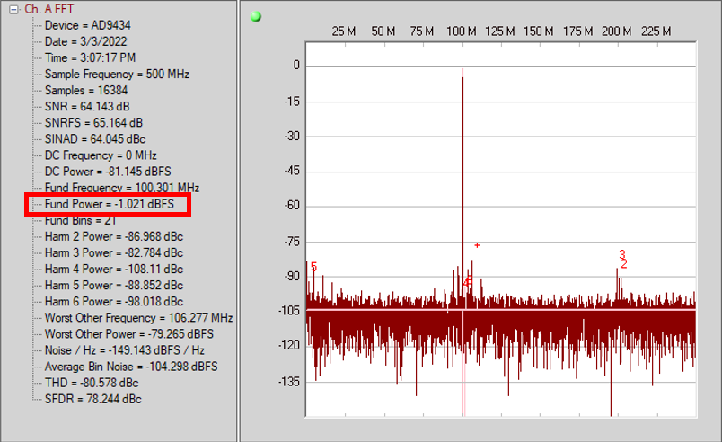
Adjust the amplitude of the input signal so that the fundamental is at -1.0 dBFS. Examine the Fund Power reading in the left panel of the VisualAnalog Graph - AD9434 Average FFT window (see Figure 14) to verify this.
Click the disk icon within the Graph window to save the performance plot data as .csv formatted file.
Testing Additional AD9434 Boards
Power down the EVAL-SDP-CH1Z SDP-H1 board first before swapping them.
Considerations on the Use of Different Clock Configurations
This section is created to give highlight on the capability of AD9434-FMC-500EBZ board to cater different clock circuitries and its performance at maximum sample rate of 500MSPS. The board itself has provisions for external signal generator, oscillator, LVPECL, and LVDS. For oscillator, the board uses CCS575S Crystek SAW clock oscillator. For LVPECL and LVDS, AD9517-4 is leveraged as clock buffer using internal VCO with clock distribution mode.
SNR Performance of AD9434
With reference to an-501 and an-756, the SNR performance as shown in Figure 17 gives insight on the effect of clock jitter to the AD9434’s signal-to-noise ratio (SNR) performed in evaluation board clock set-up depicted in Figure 16. The external signal generator clock circuitry provides the best performance among other clock configurations, which uses Rhode and Schwarz SMA100B. The CCS575S oscillator ranks second in terms of SNR performance, followed by LVPECL with voltage swing 960mVpp, then LVDS with 3.5mA current set-up. Both LVPECL and LVDS clock configurations were leveraged by ad9517-4. As an implication, the external signal generator has the lowest clock jitter among others.
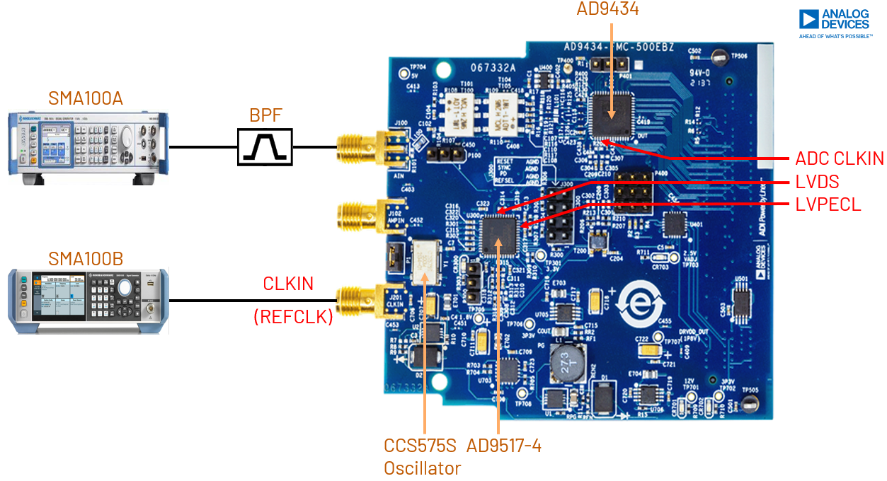
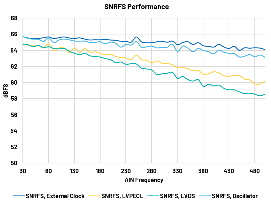
Figure 17 AD9434 SNR Performance using Different Clock Configurations
As a trade-off in getting the best SNR performance, the material cost and resources are higher for external signal generator clock configuration. However, the user can get a better performance (almost -1 dB less than the external signal generator) with optimized material cost in oscillator clock configuration using CCS575S. For the lowest material cost compared to oscillator, the ad9517-4 can offer a good functionality in using either LVPECL or LVDS configurations. In design considerations, the user should get a good balance between ease of resources and ADC performance.
Component Alteration for different Clock Configurations
This section is created to be a guide on how to rework the AD9434-FMC-500EBZ board to the desired user clock circuitry.
Clock Configuration |
Install |
Uninstall |
|---|---|---|
External Signal Generator |
as is |
as is |
Oscillator |
R209, P1(shunt) |
None |
LVPECL |
R208, R307, R308, C300, C311, C304, C305 |
C209, C210 |
LVDS |
R208, C306, C307 |
C209, C210, R311 |
For LVPECL and LVDS configurations, appropriate charge pump filter circuit values are necessary to have an optimized clock buffer performance from ad9517-4. The user can get appropriate values by simulating the ad9517-4 from ADIsimCLK.
How to use SPIController for AD9517-4 Register Setting
After configuring the SPIController for AD9434 using FIFO Select 1, this section shows how to configure the SPIController by writing and reading values in ad9517-4. Below are the following steps:
Start another SPIController
If a pop-up message saying “Read Test Failure”, select**Ignore**.
Click File > Cfg Open, then find a file named “AD9517spiR03.cfg” and double click it.
Again, if a message pop up saying “Read Test Failure”, select again Ignore.
Click Config > Controller Dialog.
Click FIFO Chip Sel# and choose 2, and unselect SDO Active then click OK.
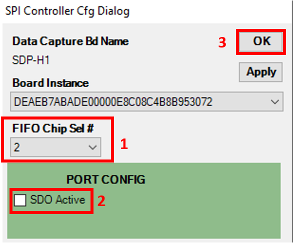
Figure 22 Configuring the FIFO Chip Select in Controller Dialog Section
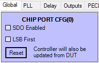
Go to Global tab and click Reset.
Configure the PLL tab of the SPIController to the user desired settings.
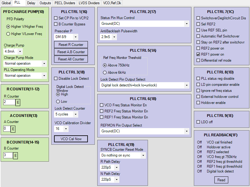
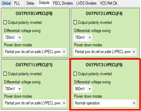
For the Output tab, the user can select on either LVPECL or LVDS. For LVPECL clock path connected to ad9434, configure Output3 LVPECL(0x0F5), and set the differential voltage swing and the power modes to Normal Operation. For the rest of LVPECL outputs, set them to Safe LVPECL power-down, and also check the Power-down Output of all the LVDS outputs.
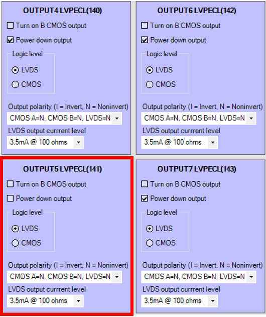
For LVDS clock path connected to ad9434, configure the Output5 (0x141) by unchecking the power-down output with output polarity of CMOS = A, CMOS B = N, LVDS = N and setting the LVDS output current level to 3.5mA at 100 ohms and all the LVPECL outputs to Safe LVPECL power-down.
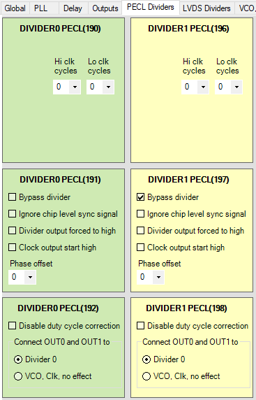
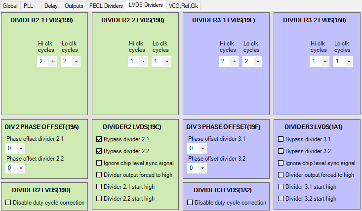
Configure the desired LVPECL divider settings shown in Figure 27 or configure the desired LVDS divider settings shown in Figure 28.
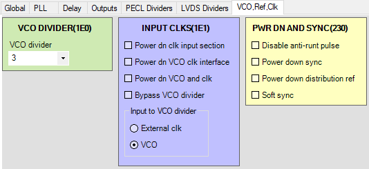
For internal VCO mode, configure the VCO divider to desired value and set the Input to VCO divider to VCO.
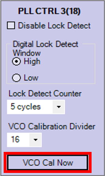
After setting the desired register addresses, go back to PLL tab specifically the PLL CTRL 3 (0x18) and click the VCO Cal Now.
Click the Update DUT from Controller in the icon shown in Figure 31 and wait if the LED CR300 will lit up. Insert a REFCLK in J201 in order for the PLL in the ad9517-4 to lock.
Go back to VisualAnalog and see if the user can produce an FFT using the desired clock configuration using ad9517-4.
Troubleshooting Tips
If the FFT plot appears abnormal, do the following:
If you see a normal noise floor when you disconnect the signal generator from the analog input, be sure you are not overdriving the ADC. Reduce the input level, if necessary.
In VisualAnalog, click the Settings button in the Input Formatter block. Check that Number Format is set to correct encoding (offset binary by default).
If the FFT appears normal but the performance is poor, check the following:
Make sure that an appropriate band-pass filter is used on the analog input.
Make sure that the signal generators for the clock and the analog input are clean (low phase noise).
Change the analog input frequency slightly if noncoherent sampling is being used, or use coherent frequencies.
Make sure that the SPI configuration file matches the product being evaluated.
Make sure the there isn’t any extra stress/torque on the clock and analog input connectors.
If the FFT window remains blank after Run is clicked, do the following:
Make sure that the evaluation board is securely connected to the EVAL-SDP-CH1Z SDP-H1 board.
Make sure that the FPGA has been programmed by verifying that the FPGA_DONE LED is illuminated on the EVAL-SDP-CH1Z board. If this LED is not illuminated, reprogram the FPGA through VisualAnalog. If the LED still does not illuminate, disconnect the USB and power cord for 15 seconds. Connect again and repeat the SDP-H1 setup process.
Make sure the correct FPGA bin file was used to program the FPGA.
Be sure that the correct sample rate is programmed. Click on the Settings button in the ADC Data Capture block in VisualAnalog and verify that he Clock Frequency is properly set.
Ensure that the ADC has valid clock input.
If the FFT appears normal but the analog input frequency is not matched in VA compared to the AIN input source, do the following: