User guide
Warning
The AD-FMCADC5-EBZ is a legacy product and is no longer actively supported. This documentation is provided for reference only.
Hardware guide
Specifications
The AD-FMCADC5-EBZ board’s primary purpose is to quickly and easily connect to an FMC carrier platform and start collecting data using the two AD9625 devices. The board is a double FMC wide board and requires two fully populated (transceivers mainly) FMC connectors on the carrier (such as VC707). The board is designed to be easy to use. Out of the box the board will self power and self clock when connected to an FMC carrier. The analog signal input is connected to J18.
The AD-FMCADC5-EBZ uses a 2.5 GHz crystal. The two AD9625 devices are clocked from the same clock source, but 180 degrees out of phase to each other. This 180-degree phase offset is what enables the effective 5 GSPS interleaved sampling rate: the first ADC samples at the rising edges of the 2.5 GHz clock, while the second ADC samples at the falling edges.
The analog signal is connected to the board at connector J18. The board is designed for a wide bandwidth input to allow high frequency RF signals to be captured effectively.
A calibration signal connector (J15) is also available as an alternative input for HDL-based calibration of the interleaving order.
Software guide
FPGA Code
The AD-FMCADC5-EBZ HDL reference design is built around a MicroBlaze processor as in an embedded system. Library cores used:
No-OS Software
The AD-FMCADC5-EBZ No-OS software source can be found at fmcadc5 project.
Running No-OS Application
The HDL reference design is built around a processor as in an embedded system. You may use either Linux or No-OS software to demonstrate the design. In order to run the HDL with the No-OS application, one needs to build the HDL bit file and software elf file. The Build an HDL project contains the instructions to build the bit file.
Once the bit file is ready, follow these instructions to build the elf file. This assumes you are following our directory structures.
Clone No-OS repository
Checkout the 2018_R1 release branch (
git checkout 2018_R1)Change the directory to
fmcadc5/vc707.Make the elf file by running
make HDF-FILE=<HDL-REPO>/projects/fmcadc5/vc707/fmcadc5_vc707.sdk/system_top.hdf
A typical run looks like this:
[~/github/noos/ad-fmcadc5-ebz/vc707]> make HDF-FILE=~/github/hdl/projects/fmcadc5/vc707/fmcadc5_vc707.sdk/system_top.hdf
xsct -s ../../scripts/xilinx_xsct.tcl ~/github/hdl/projects/fmcadc5/vc707/fmcadc5_vc707.sdk/system_top.hdf >> xilinx_xsct.log 2>&1

mb-gcc -Wall -mlittle-endian -mxl-soft-mul -mcpu=v9.2 -mxl-soft-mul -DXILINX -Ibsp/sys_mb/include -I.. -I../../common_drivers/xilinx_platform_drivers -I../../common_drivers/jesd204b_gt -I../../common_drivers/jesd204b_v51 -I../../common_drivers/adc_core -I../../drivers/ad9625 -Os -ffunction-sections -fdata-sections -o vc707.elf sw/src/platform.c ../ad_fmcadc5_ebz.c ../../common_drivers/xilinx_platform_drivers/platform_drivers.c ../../common_drivers/jesd204b_gt/jesd204b_gt.c ../../common_drivers/jesd204b_v51/jesd204b_v51.c ../../common_drivers/adc_core/adc_core.c ../../drivers/ad9625/ad9625.c -Lbsp/sys_mb/lib/ -Tsw/src/lscript.ld -Wl,--start-group,-lxil,-lgcc,-lc,--end-group
Start an UART terminal.
port    = /dev/ttyUSB0
speed   = 115200
bits    = 8
stopbits    = 1
parity  = none
crlfauto    = True ## if not set, expect non-aligned text

[~/github/noos/ad-fmcadc5-ebz/vc707]> gtkterm -c USB0 &
The folder contains a vc707.tcl file that you can launch with xmd. It can be also run using Vivado or SDK.
[~/github/noos/ad-fmcadc5-ebz/vc707]> xmd -tcl vc707.tcl
rlwrap: warning: your $TERM is 'xterm' but rlwrap couldn't find it in the terminfo database. Expect some problems.

* Xilinx Microprocessor Debugger (XMD) Engine
* XMD v2015.2 (64-bit)
*** SW Build 1266856 on Fri Jun 26 16:35:25 MDT 2015
   ** Copyright 1986-2015 Xilinx, Inc. All Rights Reserved.

Executing user script : vc707.tcl
Configuring Device 1 (xc7vx485t) with Bitstream -- hw/system_top.bit
..............................10..............................20..............................30......................................................10..............................20..............................30......................................................10..............................20..............................30......................................................10..............................20..............................30......................................................10..............................20..............................30..............................40..............................50..............................60..............................70..............................................10..............................20..............................30..............................40..............................50..............................60..............................70..............................................10..............................20..............................30..............................40..............................50..............................60..............................70..............................80..............................90..............................Done
Successfully downloaded bit file.

JTAG chain configuration
Device   ID Code        IR Length    Part Name
1       23687093           6        xc7vx485t

JTAG chain configuration
Device   ID Code        IR Length    Part Name
1       23687093           6        xc7vx485t

MicroBlaze Processor Configuration :
Version............................9.5
Optimization.......................Performance
Interconnect.......................AXI-LE
MMU Type...........................Full_MMU
No of PC Breakpoints...............1
No of Read Addr/Data Watchpoints...0
No of Write Addr/Data Watchpoints..0
Instruction Cache Support..........on
Instruction Cache Base Address.....0x80000000
Instruction Cache High Address.....0xbfffffff
Data Cache Support.................on
Data Cache Base Address............0x80000000
Data Cache High Address............0xbfffffff
Exceptions  Support................on
FPU  Support.......................off
Hard Divider Support...............on
Hard Multiplier Support............on - (Mul64)
Barrel Shifter Support.............on
MSR clr/set Instruction Support....on
Compare Instruction Support........on
PVR Supported......................on
PVR Configuration Type.............Full
Data Cache Write-back Support......off
Fault Tolerance Support............off
Stack Protection Support...........off

Connected to "mb" target. id = 0
Starting GDB server for "mb" target (id = 0) at TCP port no 1234
Processor stopped

System Reset .... DONE
Downloading Program -- vc707.elf
      section, .vectors.reset: 0x00000000-0x00000007
      section, .vectors.sw_exception: 0x00000008-0x0000000f
      section, .vectors.interrupt: 0x00000010-0x00000017
      section, .vectors.hw_exception: 0x00000020-0x00000027
      section, .text: 0x80000000-0x800069fb
      section, .init: 0x800069fc-0x80006a2f
      section, .fini: 0x80006a30-0x80006a4b
      section, .ctors: 0x80006a4c-0x80006a53
      section, .dtors: 0x80006a54-0x80006a5b
      section, .rodata: 0x80006a5c-0x8000723f
      section, .data: 0x80007240-0x8000746f
      section, .eh_frame: 0x80007470-0x800074fb
      section, .jcr: 0x800074fc-0x800074ff
      section, .bss: 0x80007500-0x8000762b
      section, .heap: 0x8000762c-0x80007a2f
      section, .stack: 0x80007a30-0x80007e2f
Download Progress..10.20.30.40.50.60.70.80.90.Done
Setting PC with Program Start Address 0x00000000
Processor started. Type "stop" to stop processor

RUNNING> Disconnected from Target 0

[~/github/noos/ad-fmcadc5-ebz/vc707]>
The following messages should appear on the terminal.
AD9625 successfully initialized.
AD9625 successfully initialized.
JESD204B successfully initialized.
JESD204B successfully initialized.
SYSREF Calibration Successful[4]
ADC Core Initialized (157 MHz).
ADC Core Initialized (157 MHz).
Initialization done.
Capture done.
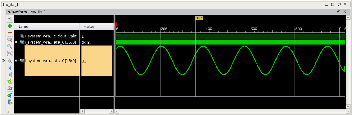
This should appear on the ILA:
Interleaving
Interleaving (HDL)
As a brief introduction to interleaving: there are two AD9625 devices running at 2.5 Gbps, with clocks that are 180 degrees out of phase. The input signal is sampled by the first ADC at the rising edges of the 2.5 GHz clock and by the second ADC at the falling edges of the conceptually same clock, yielding an effective sampling rate of 5 GSPS. The two sample streams then need to be interleaved. That sounds straightforward, but there are some challenges.
A note of caution: this interleaving approach inherently introduces performance factors that are outside the scope of this discussion. The two main factors are jitter on the sampling clocks and gain/phase variations at the input. The devices may also have encoding skew, some of which can be filtered or compensated by post-processing.
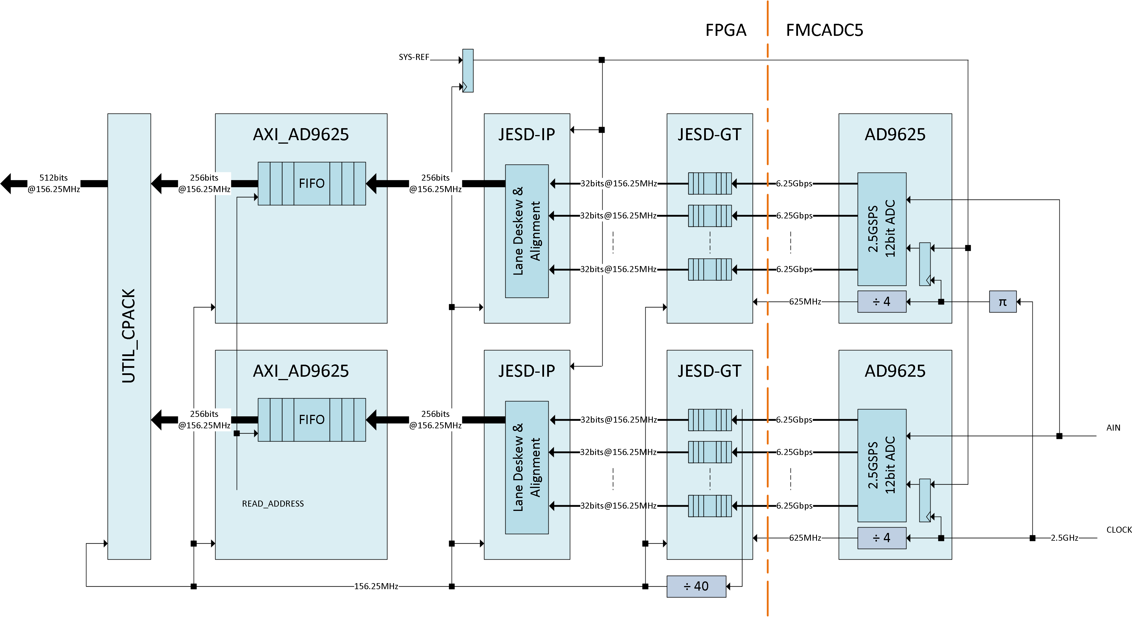
Examining the data path of the devices independently (see block diagram above), alignment and deskew occur at various stages. The transceivers perform deskew and alignment of bits (comma character alignment and 10B to 8B conversion). The JESD-IP then aligns individual lanes and outputs data with a fixed latency using SYSREF. The SYSREF resets the LMFC, so the receiver can determine the system latency from the time it receives the SYSREF pulse to the first received ILA data. After this, the samples reach the AD9625 core.
Each core receives two samples per device. Determining which sample comes first in time is essential because the samples must be interleaved in the exact order they were captured. In theory, JESD204B subclass-1 operation with SYSREF should be sufficient for this. SYSREF is the absolute time reference for all transmit and receive devices involved. In practice, however, SYSREF is rarely used as a clock. It is treated as data and sampled by each device at its own clock. A more robust approach is to identify, at the receiving device, the exact sample at which SYSREF was captured. The AD9625 supports a mode that attaches a time stamp to the samples - details are in the data sheet. The FPGA design uses this time stamp to determine the exact sample at which each device captured SYSREF. It does so by aligning samples across the 16-sample data output per device per clock, then writing data to a small FIFO whose write pointer is reset by the SYSREF time stamp. A common read pointer reads the samples back out. The FIFO supports deskewing of up to 8 samples. The ADC pack interleaves these samples assuming device-0 is first in order. The software must ensure that device-0 always samples SYSREF half a clock ahead of device-1, which is achieved through a calibration routine.
Note
The AD9625 supports time stamp insertion at the LSB of the sample (and is the ONLY option in certain lane configurations). This changes the devices to 11-bit converters. The HDL design does NOT support this. It supports time stamp insertion in the CS bits ONLY. The converter resolution remains as 12-bit. If you would prefer the LSB option, you need to change both HDL and software.
Interleaving (SW)
The software programs both the devices and the GPIO, transceivers and IP cores in the FPGA. The default transceiver setup only supports single-chip, single-link configuration. It also does not take into account that a single SYSREF controls both the devices and transceivers. The default routine is therefore modified to leave the transceivers up and running but the data path is held under reset. This is required because the AD9625 does NOT always wait for SYSREF to start the ILA phase after CGS. The second SYSREF may reset the LMFC, but in its absence, ILA phase is initiated.
This is the section of the code where the initial setup is done:
if (adc5_gpio_ctl(GPIO_DEVICE_ID))
  return -1;

ad9625_setup(XPAR_SPI_0_DEVICE_ID, 0);
ad9625_setup(XPAR_SPI_0_DEVICE_ID, 1);

jesd204b_gt_initialize(XPAR_AXI_FMCADC5_0_GT_BASEADDR, 8);
jesd204b_setup(XPAR_AXI_AD9625_0_JESD_BASEADDR, jesd204b_st);
jesd204b_gt_setup_modified(jesd204b_gt_link);

jesd204b_gt_initialize(XPAR_AXI_FMCADC5_1_GT_BASEADDR, 8);
jesd204b_setup(XPAR_AXI_AD9625_1_JESD_BASEADDR, jesd204b_st);
jesd204b_gt_setup_modified(jesd204b_gt_link);
The devices need to be re-programmed to support interleaving. The sequence below enables the SYSREF time stamping in the CS bits and also programs the monitoring of SYSREF signals for setup/hold violations at the 2.5 GHz clock. This is required to ensure that the sampling order is correct.
ad9625_spi_write(0, 0x072, 0x8b);
ad9625_spi_write(0, 0x03a, 0x02);
ad9625_spi_write(0, 0x0ff, 0x01);
ad9625_spi_write(1, 0x072, 0x8b);
ad9625_spi_write(1, 0x03a, 0x02);
ad9625_spi_write(1, 0x0ff, 0x01);
If starting from reset, the devices are in CGS at this time. The AD9625 may initiate a ILA as soon as it sees SYNC deasserted regardless of SYSREF. So we need to make sure that the link is down and the data path is in reset before synchronization. The following routine resets the data path and keeps SYNC asserted (SYSREF is NOT active):
gtlink_control(0);
if (gtlink_sysref(0, 0xffff) != 0) {
  xil_printf("[%05d]: Interleaving Synchronization Failed, Exiting!!\n", __LINE__);
  return(-1);
}
The following routine brings the data path out of reset and deasserts SYNC. The SYSREF is set and status is checked for all data lanes to be active and in SYNC:
gtlink_control(1);
if (gtlink_sysref(1, 0x1ffff) != 0) {
  xil_printf("[%05d]: Interleaving Synchronization Failed, Exiting!!\n", __LINE__);
  return(-1);
}
The software calibration essentially moves in and out of these two routines each time making sure that SYSREF is sampled by the devices in order. Device-0 samples SYSREF at its rising edge (the rising edge of the “conceptual clock”), device-1 samples SYSREF at its rising edge after that (the falling edge of the “conceptual clock”). The software moves the SYSREF until it sees a violation on the signal by device-0 but NOT device-1. The setup window is set such that this still does NOT cause an actual violation so that device-0 samples the signal correctly.
ad9625_sysref_sw_calibrate();
After calibration, the software brings the cores out of reset. As a measure of the link status, it monitors the PRBS sequences and makes sure that they were synchronized between the devices and the cores:
adc_setup(ad9625_0, 1);
adc_setup(ad9625_1, 1);

ad9625_spi_write(0, AD9625_REG_TEST_CNTRL, 0x5);
ad9625_spi_write(0, AD9625_REG_OUTPUT_MODE, 0x0);
ad9625_spi_write(0, AD9625_REG_TRANSFER, 0x1);

ad9625_spi_write(1, AD9625_REG_TEST_CNTRL, 0x5);
ad9625_spi_write(1, AD9625_REG_OUTPUT_MODE, 0x0);
ad9625_spi_write(1, AD9625_REG_TRANSFER, 0x1);

if (adc_pn_mon(ad9625_0, 1, ADC_PN23A) != 0) return(-1);
if (adc_pn_mon(ad9625_1, 1, ADC_PN23A) != 0) return(-1);
The devices are set to disable the test patterns and data format is set to 2’s complement with sign extension. The ILA core is 16-bit samples and the format must be signed decimal to display analog signal correctly:
ad9625_spi_write(0, AD9625_REG_TEST_CNTRL, 0x0);
ad9625_spi_write(0, AD9625_REG_OUTPUT_MODE, 0x1);
ad9625_spi_write(0, AD9625_REG_TRANSFER, 0x1);
adc_write(ad9625_0, ADC_REG_CHAN_CNTRL(0), 0x51);

ad9625_spi_write(1, AD9625_REG_TEST_CNTRL, 0x0);
ad9625_spi_write(1, AD9625_REG_OUTPUT_MODE, 0x1);
ad9625_spi_write(1, AD9625_REG_TRANSFER, 0x1);
adc_write(ad9625_1, ADC_REG_CHAN_CNTRL(0), 0x51);
ILA
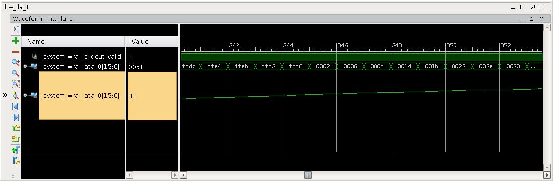
The design instantiates an ILA core that serializes the interleaved 512 samples per clock down to 1 sample per clock, allowing the interleaving order to be inspected directly. The following captures illustrate correct operation:
ILA waveform overview.
Sine wave zoomed between -1 and 1.
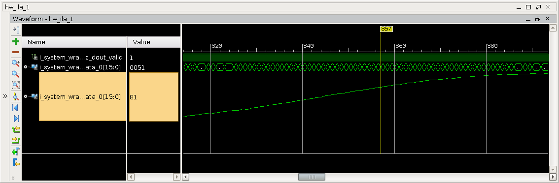
Values zoomed in — all samples are in strictly increasing order.
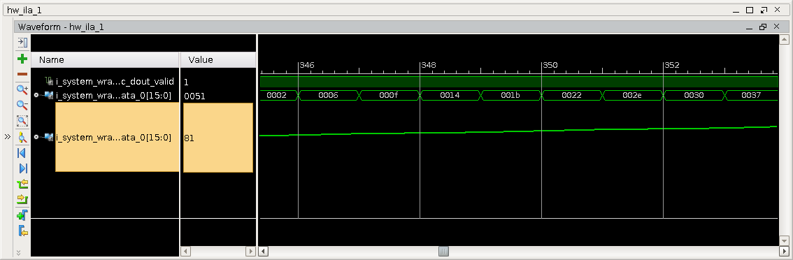
Zero crossing region with values zoomed in — samples remain in increasing order.
To observe the effect of an interleaving order violation, the calibration function can be replaced or followed by the routine below, which forces a violation:
while (1) {
   gtlink_control(0);
   if (gtlink_sysref(0, 0xffff) != 0) {
     xil_printf("[%05d]: Interleaving Synchronization Failed, Exiting!!\n", __LINE__);
     return(-1);
   }

   gtlink_control(1);
   if (gtlink_sysref(1, 0x1ffff) != 0) {
     xil_printf("[%05d]: Interleaving Synchronization Failed, Exiting!!\n", __LINE__);
     return(-1);
   }

   if (ad9625_sysref_status() != 0) break;
}
When the violation is triggered, the ILA captures will show samples out of order:
ILA waveform overview.
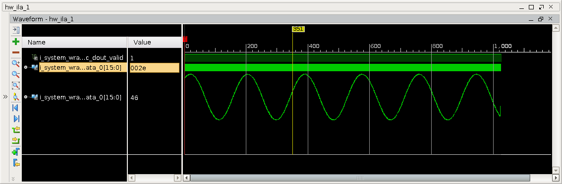
Sine wave zoomed between -1 and 1 — a “saw-tooth” artifact is visible due to out-of-order samples.
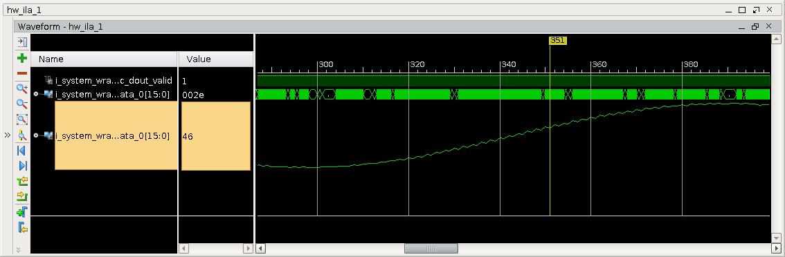
Values zoomed in — alternating samples are swapped, but each subsequence individually maintains increasing order.
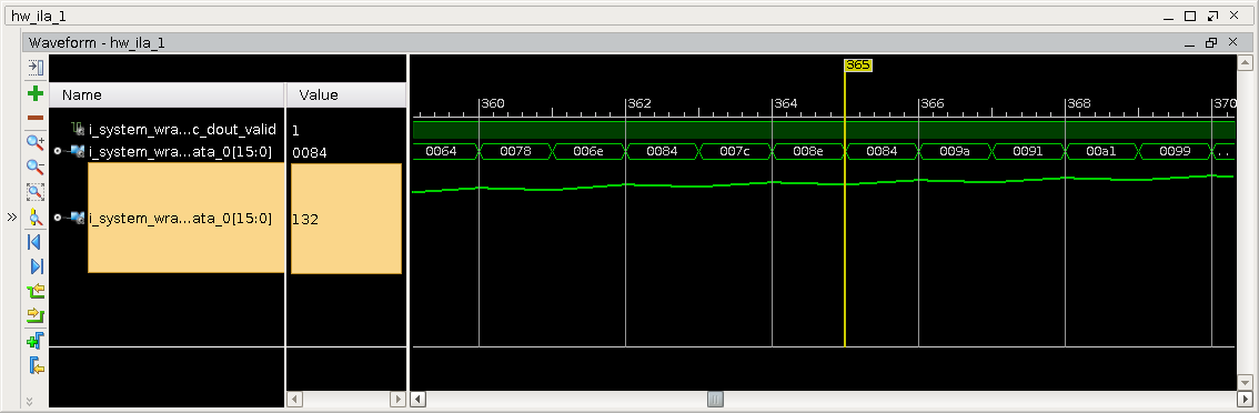
Zero crossing region with values zoomed in — alternating samples are out of order.
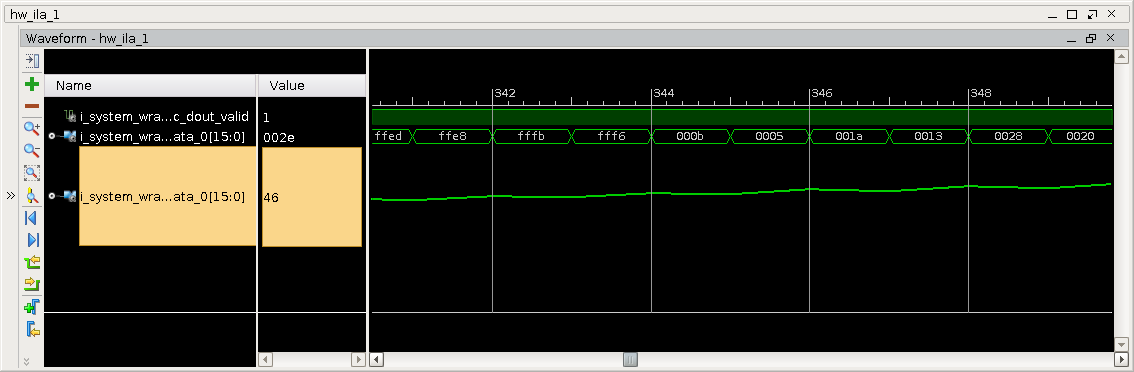
The same behavior is observable at higher input frequencies:
~900 MHz input.
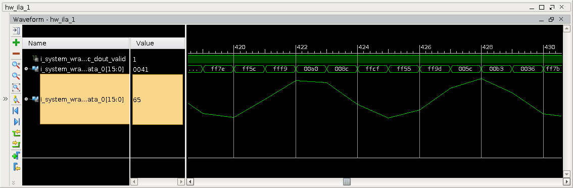
~66 MHz input.
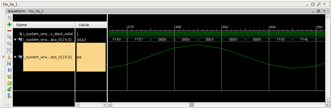
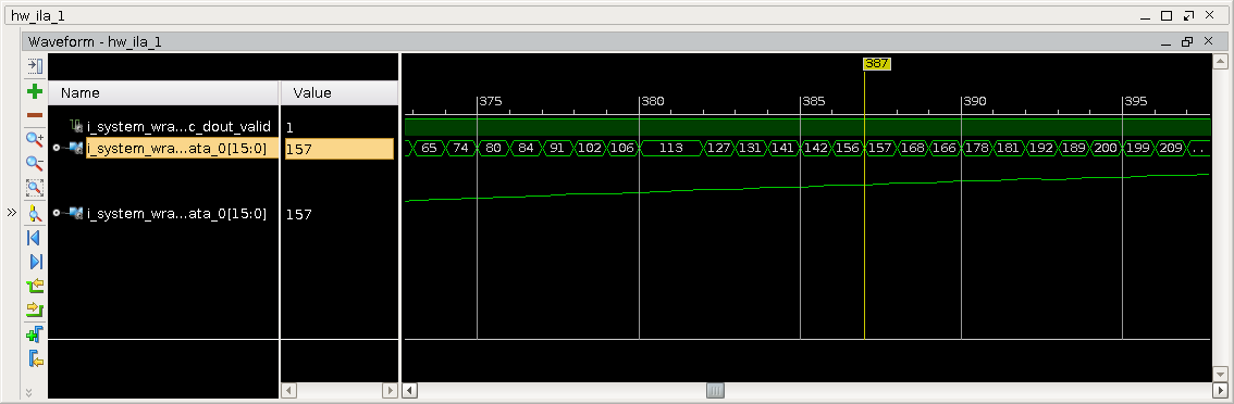
When interleaving order is correct, the output may still appear misaligned due to offset and gain differences between the two ADCs. This effect is less pronounced when the input gradient is high, but is clearly visible at signal peaks. The following captures show correct interleaving order:
Interleaved signal.
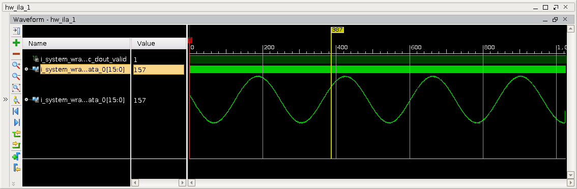
Zoom in the window below.
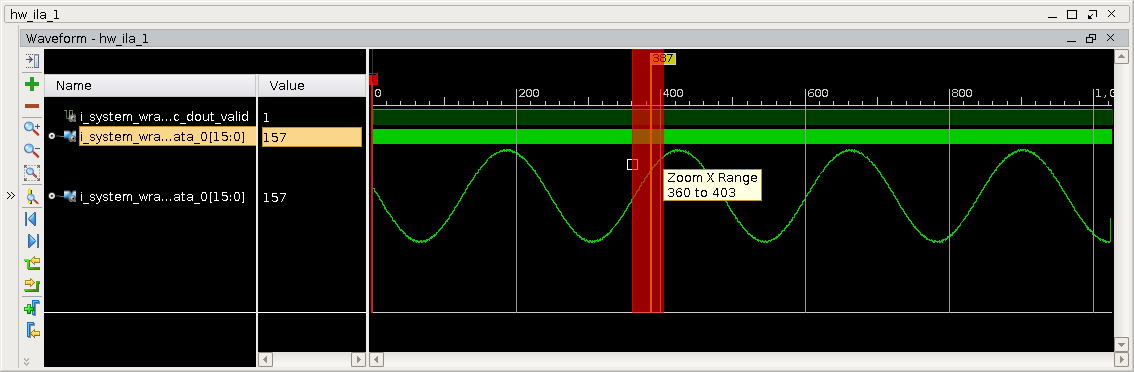
The samples are in order.
Zoom in the window at the peak below.
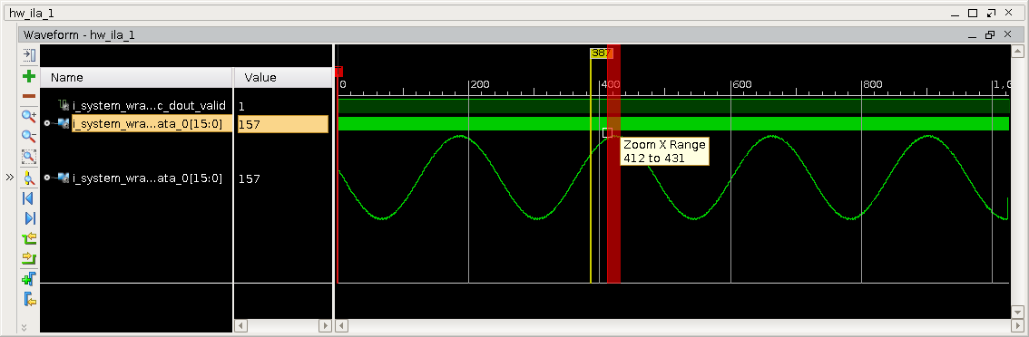
The samples are in order, but appear to be out of order.
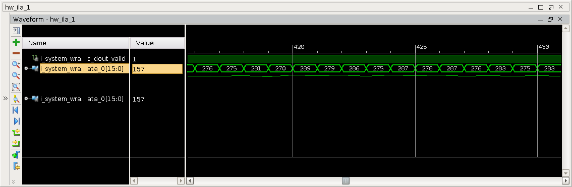
Figure 17 Samples appear out of order at peak due to offset/gain differences
Linux
Help & Support
Hint
Build an HDL project contains all the documentation, build instructions and register map tables.
Browse the HDL GitHub repository: library components and projects.
Questions? Ask on FPGA questions, Linux driver questions, or No-OS Drivers questions.