User guide
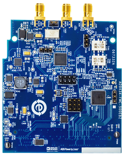
EVAL-AD9434 top view:
Hardware guide
Hardware configuration - Clock Scheme
There are multiple ways to configure the clock source for AD9434. In this section is presented a guide on how to rework the board to the desired user clock circuitry. Below is a table on what components are needed to install or uninstall on the evaluation board.
Clock Configuration |
Install |
Uninstall |
|---|---|---|
Ext. Signal Gen. |
as it is |
as it is |
Oscillator |
R209, P1(shunt) |
— |
LVPECL |
R208, R307, R308, C300, C311, C304, C305 |
C209, C210 |
LVDS |
R208, C306, C307 |
C209, C210, R311 |
For LVPECL and LVDS configurations, appropriate charge pump filter circuit values are necessary to have an optimized clock buffer performance from AD9517-4.
Warning
On Zedboard, the frequency is set to 463.82MHz, because there is a limitation for BUFG input clock frequency to 464MHz, which is below the maximum sampling rate of the ADC (500MSPS).
Thus the adc_clk period is set to 2.156ns (463.82MHz) on Zedboard.
Power supply
The power supply comes from the FMC connector, given by the FPGA.
The VADJ values can be checked out in the README.md file of each combination with an FPGA, at: projects/ad9434_fmc.
Software guide
The evaluation board is supported with the Libiio library. This library is cross-platform (Windows, Linux, Mac) with language bindings for C, C#, Python, MATLAB, and others. Two easy examples that can be used with it are: