EVAL-AD9083
16-Channel, 125 MHz Bandwidth, Continuous Time Σ-Δ ADC.
Overview
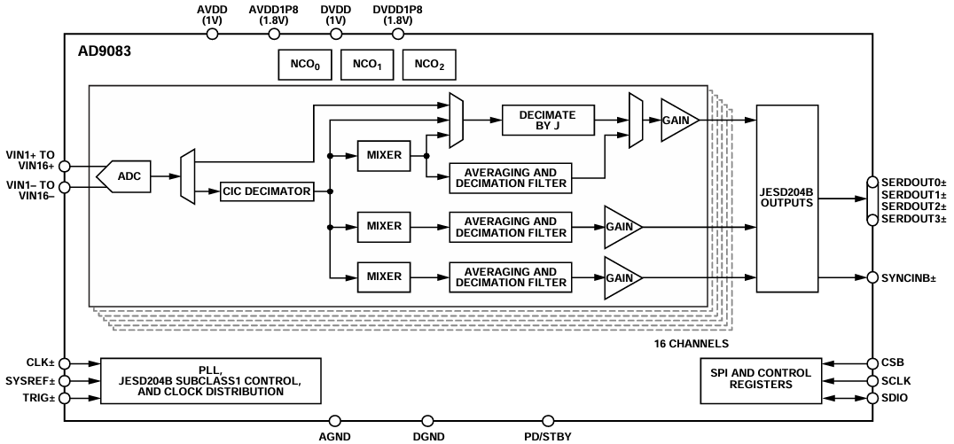
The EVAL-AD9083 is an FMC evaluation card for the AD9083, a 16-channel, 125 MHz bandwidth, continuous time Σ-Δ (CTSD) ADC. The device features an on-chip, programmable, single-pole antialiasing filter and termination resistor designed for low power, small size, and ease of use.
Each of the 16 ADC cores features a first-order CTSD modulator architecture with integrated, background nonlinearity correction logic and self-cancelling dither. Each ADC has a signal processing tile to filter out-of-band shaped noise and reduce the sample rate, containing a cascaded integrator comb (CIC) filter and a quadrature digital downconverter (DDC) with multiple finite input response (FIR) decimation filters.
The serialized output uses a Subclass 1 JESD204B interface configurable in various lane configurations (up to four lanes). Multiple device synchronization is supported through the SYSREF±, TRIG±, and SYNCINB± input pins.
Features:
16-channel, 125 MHz bandwidth CTSD ADC
Programmable single-pole antialiasing filter
Programmable input termination resistor
Integrated background nonlinearity correction and self-cancelling dither
Signal processing tile per channel: CIC filter + quadrature DDC + FIR
JESD204B interface, up to 4 lanes (Subclass 1)
Multiple device synchronization (SYSREF±, TRIG±, SYNCINB±)
1.8 V SPI (3-wire) configuration interface
Flexible power-down modes
100-ball CSP_BGA, −40°C to +85°C
Applications:
Multi-channel instrumentation and data acquisition
Phased array radar and electronic warfare
Test and measurement equipment
Communications receivers
Medical imaging
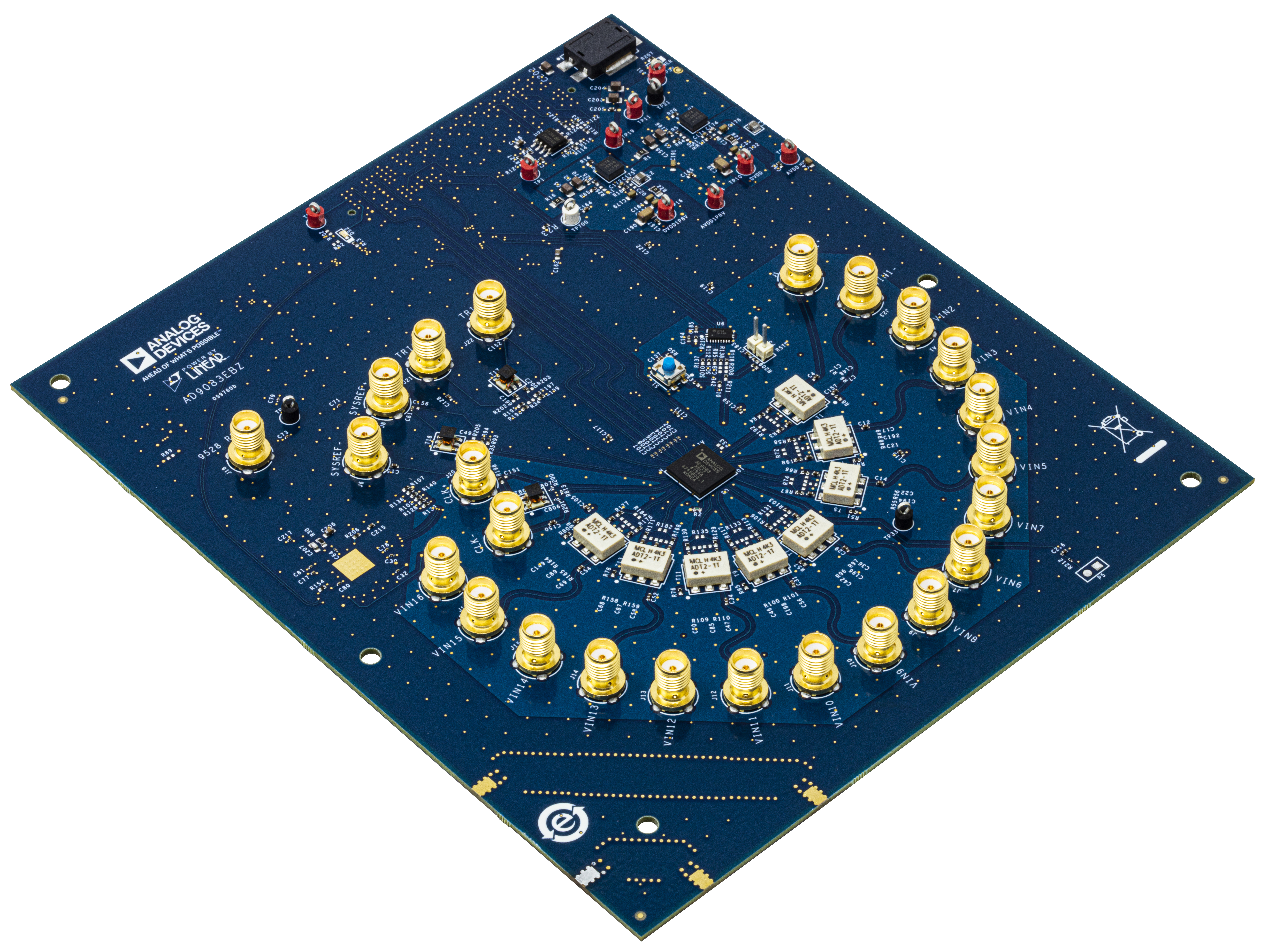
EVAL-AD9083 looks like this:
Recommendations
People who follow the flow that is outlined, have a much better experience with things. However, like many things, documentation is never as complete as it should be. If you have any questions, feel free to ask on our EngineerZone forums, but before that, please make sure you read our documentation thoroughly.
To better understand the AD9083, we recommend using the EVAL-AD9083 evaluation board.
Table of contents
Using the evaluation board/full stack reference design that we offer:
Prerequisites — what you need to get started
-
Using the ZCU102/Zynq UltraScale+ MP SoC
Configure an SD Card with Kuiper
Linux Applications
Design with the AD9083
Resources for designing a custom AD9083-based platform software
For Linux software:
About the device driver:
About the JESD204 utilities:
HDL reference design which you must use in your FPGA.
Block diagram
ADI articles
About the JESD204 standard:
Warning
All the products described on this page include ESD (electrostatic discharge) sensitive devices. Electrostatic charges as high as 4000V readily accumulate on the human body or test equipment and can discharge without detection. Although the boards feature ESD protection circuitry, permanent damage may occur on devices subjected to high-energy electrostatic discharges. Therefore, proper ESD precautions are recommended to avoid performance degradation or loss of functionality. This includes removing static charge on external equipment, cables, or antennas before connecting to the device.
Help and support
Please go to Help and Support page.