System Integration
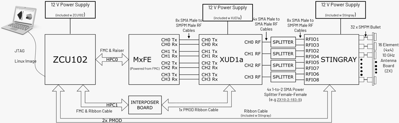
This section covers how the three main boards of the X-Band platform work together to create a complete hybrid beamforming phased array system.
System Architecture Overview
The X-Band Development Platform implements a hybrid beamforming architecture that combines:
Analog beamforming via ADAR1000EVAL1Z (32 channels)
Digital beamforming via AD9081-FMCA-EBZ (4 digital channels)
Frequency conversion via ADXUD1AEBZ (X-Band ↔ C-Band)
FPGA processing via ZCU102 (control and algorithms)
Signal Flow Architecture
Receive Path
Antenna → ADAR1000 → XUD1A → AD9081 → ZCU102
(32ch)     (32→4)    (X→C)    (4)     (Processing)
32 Antenna Elements collect RF signals at X-Band frequencies
ADAR1000 Analog Beamforming combines 8 interleaved channels into 4 subarrays
XUD1A Down Conversion translates X-Band RF to C-Band IF
AD9081 Digitization converts 4 analog IF to digital channels
ZCU102 Processing performs digital beamforming and signal processing
Transmit Path
ZCU102      → AD9081 → XUD1A → ADAR1000 → Antenna
(Processing)   (4)     (C→X)    (4→32)     (32ch)
ZCU102 Processing generates digital waveforms
AD9081 DACs convert digital signals to 4 analog IF channels
XUD1A Up Conversion translates C-Band IF to X-Band RF
ADAR1000 Power Division distributes 4 channels to 32 antenna elements
32 Antenna Elements radiate coherent X-Band signals
Subarray Architecture
Four 8:1 Subarrays
The system is organized into four subarrays with interleaved element assignments. Each subarray contains:
2x ADAR1000 ICs (8 channels total per subarray)
1x Power Splitter/Combiner (ZX10-2-183-S+)
1x XUD1A Channel for frequency conversion
1x AD9081 ADC/DAC pair for digitization
Physical Layout (antenna-facing view — ADAR1000 ICs on reverse side)
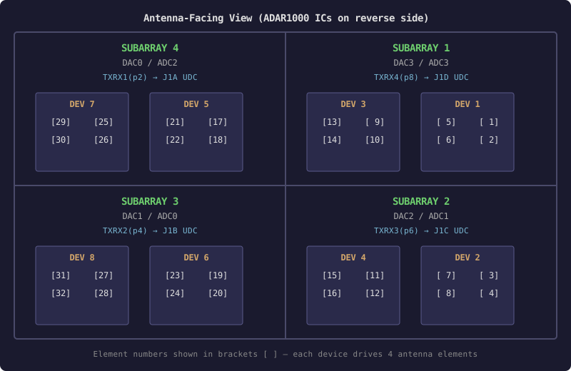
Signal Path per Subarray
Subarray |
Antenna Elements |
ADAR1000 Devices |
XUD1A Path (PMOD pin) |
AD9081 DAC / ADC |
|---|---|---|---|---|
1 |
1, 2, 5, 6, 9, 10, 13, 14 |
DEV 1, 3 |
J1D — TXRX4 (pin 8) |
DAC3 / ADC3 |
2 |
3, 4, 7, 8, 11, 12, 15, 16 |
DEV 2, 4 |
J1C — TXRX3 (pin 6) |
DAC2 / ADC1 |
3 |
19, 20, 23, 24, 27, 28, 31, 32 |
DEV 6, 8 |
J1B — TXRX2 (pin 4) |
DAC1 / ADC0 |
4 |
17, 18, 21, 22, 25, 26, 29, 30 |
DEV 5, 7 |
J1A — TXRX1 (pin 2) |
DAC0 / ADC2 |
Note
The XUD1A TX/RX direction is set via the PMOD connector’s voltage channels:
voltage1 → Subarray 4, voltage2 → Subarray 3, voltage3 → Subarray 2, voltage4 → Subarray 1.
A value of 1 selects TX (up-conversion), 0 selects RX (down-conversion).
Hybrid Beamforming Benefits
This architecture provides:
Analog beamforming: Fast, low-power steering within each subarray
Digital beamforming: Flexible, adaptive processing between subarrays
Reduced digital complexity: Only 4 digital channels vs 32
Maintained flexibility: Full beam control through combined analog/digital processing
Frequency Plan
X-Band RF Operation
Target Frequency: 10 GHz (center of X-Band)
RF Range: 8-12 GHz (X-Band)
Element Spacing: 15mm (optimized for 10 GHz)
IF Processing
IF Frequency: C-Band — recommended 4.5 GHz – 4.8 GHz between XUD1A and AD9081
LO Options: External or ADF4371 internal PLL
Default LO: Configurable based on application
IF Bandwidth: Determined by AD9081 settings
Digital Processing
ADC Sampling: Up to 4 GSPS per channel
DAC Sampling: Up to 12 GSPS per channel
Digital Channels: 8 RX, 8 TX (from 4 RF channels)
NCO Flexibility: Channel and main NCOs for fine frequency control
Control Architecture
IIO Devices
All system components are controlled through IIO (Industrial I/O) devices:
Device |
IIO Name |
Function |
|---|---|---|
ADAR1000 #1-8 |
adar1000_csb_x_x |
Analog beamforming control |
ADF4371 |
adf4371-0 |
LO generation (if used) |
AD9081 RX |
axi-ad9081-rx-hpc |
Digital receive processing |
AD9081 TX |
axi-ad9081-tx-hpc |
Digital transmit processing |
XUD1A |
xud_control |
X-Band up/down converter control |
TDD Core |
axi-core-tdd |
Time division duplexing |
Interconnect Requirements
Digital Connections
AD9081 ↔ ZCU102: FMC HPC0 connection with riser
Interposer ↔ ZCU102: FMC HPC1 connection with cable extension
Stingray ↔ ZCU102: Dual PMOD connections with adapters
RF Connections
8x SMA-SMPM cables: AD9081 ↔ XUD1A
4x Power splitters: XUD1A → splits each channel to 2 input/outputs
8x SMA-SMPM cables: Power splitters ↔ Stingray ADAR1000s
32x SMPM bullets: Stingray ADTR1107s ↔ Antenna tiles
Optional Inline Filters (recommended for improved spectral purity)
Filter |
Path |
Qty |
|---|---|---|
Mini-Circuits VLF-8400+ |
AD9081 ADC ↔ XUD1A (RX) |
4 |
Mini-Circuits VLF-5500+ |
AD9081 DAC ↔ XUD1A (TX) |
4 |
Power Distribution
ZCU102: 12V supply powers AD9081 via FMC
XUD1A: Dedicated 12V supply (~15W)
Stingray: Dedicated 12V supply (~30W)
Timing and Synchronization
Clock Distribution
Master Clock: 100 MHz reference (external or internal)
HMC7044: Clock distribution and jitter attenuation
AD9081: On-chip PLLs for ADC/DAC clocks
Phase Coherence: Maintained across all channels
TDD Coordination
TDD Engine: FPGA-based timing control
Global Sync: Coordinates all three boards
ADC/DAC Sync: Synchronized sampling and generation across all channels
Calibration Strategy
System-Level Calibration
Individual Channel Cal: Per-ADAR1000 channel calibration
Subarray Cal: Per-subarray amplitude/phase matching
Digital Cal: AD9081 channel matching
End-to-End Cal: Full system calibration via known signals
Calibration Tools
Built-in Detectors: ADAR1000 power detection
Digital Loopback: AD9081 internal test modes
External Signals: Controlled calibration sources
Over-the-Air: Pattern measurement and correction
Note
The hybrid architecture provides both the flexibility of digital beamforming and the efficiency of analog beamforming, making it ideal for radar, EW, and SATCOM applications requiring both performance and power efficiency.