AD7193 Pmod Reference Design
Introduction
The AD7193 is a low noise, complete analog front end for high precision measurement applications. It contains a low noise, 24-bit sigma-delta (Σ-Δ) analog-to-digital converter (ADC). The on-chip low noise gain stage means that signals of small amplitude can interface directly to the ADC.
The device can be configured to have four differential inputs or eight pseudo differential inputs. The on-chip channel sequencer allows several channels to be enabled simultaneously, and the AD7193 sequentially converts on each enabled channel, simplifying communication with the part. The on-chip 4.92 MHz clock can be used as the clock source to the ADC or, alternatively, an external clock or crystal can be used. The output data rate from the part can be varied from 4.7 Hz to 4.8 kHz.
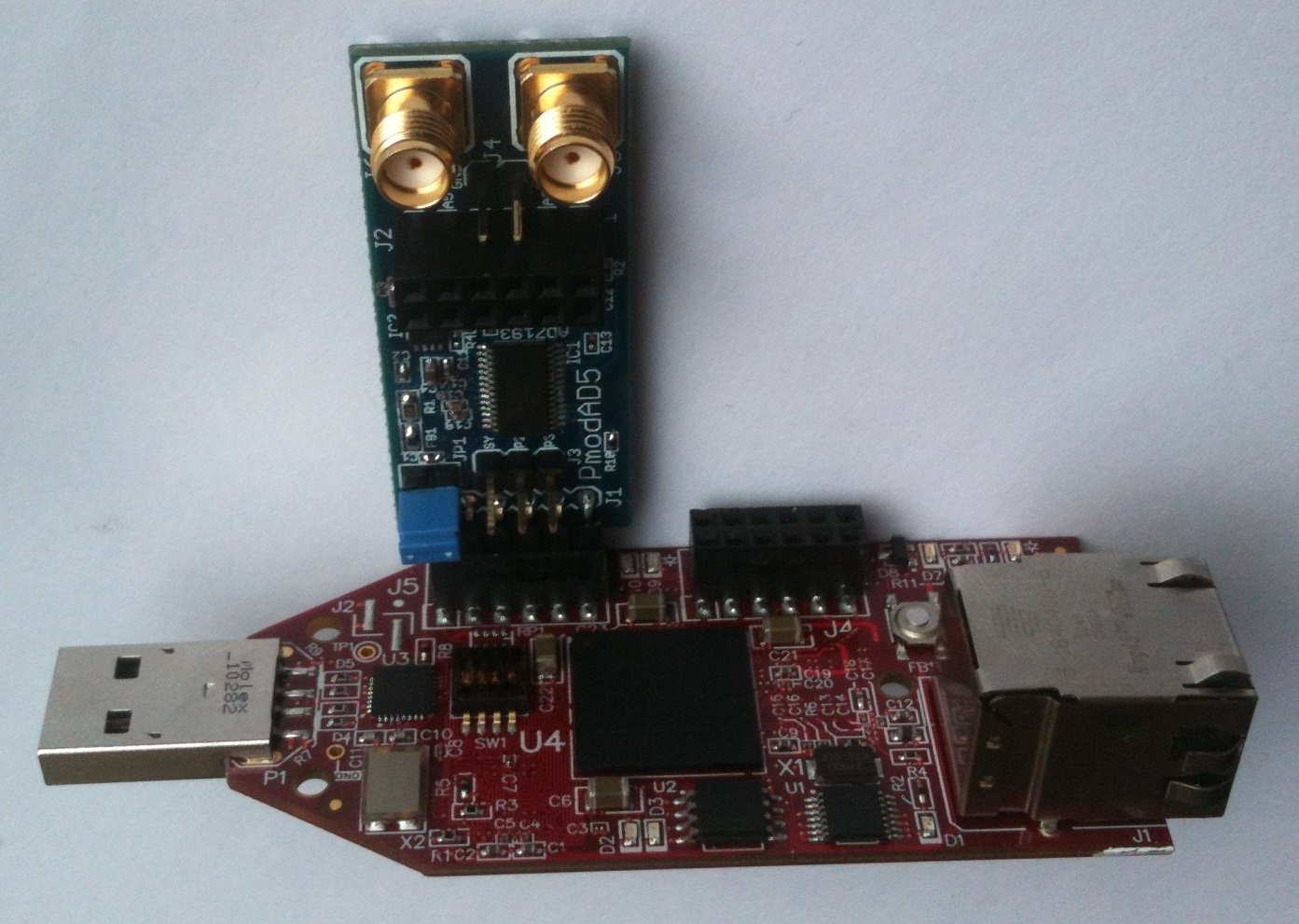
This page describes the FPGA reference design for the AD7193, using the PmodAD5 (Digilent) module connected to supported FPGA boards via the Pmod interface.
Applications
PLC/DCS analog input modules
Data acquisition
Strain gage transducers
Pressure measurement
Temperature measurement
Flow measurement
Weigh scales
Chromatography
Medical and scientific instrumentation
Supported Hardware Platforms
Spartan-6 LX9 MicroBoard (Avnet)
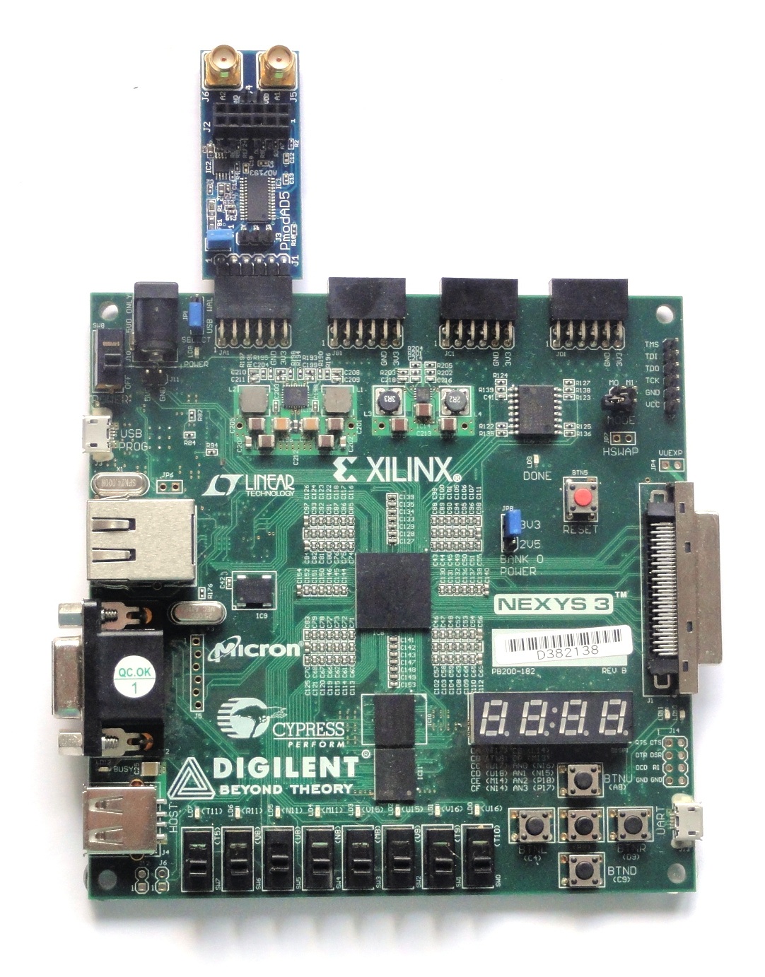
Nexys3 Spartan-6 FPGA Board (Digilent)
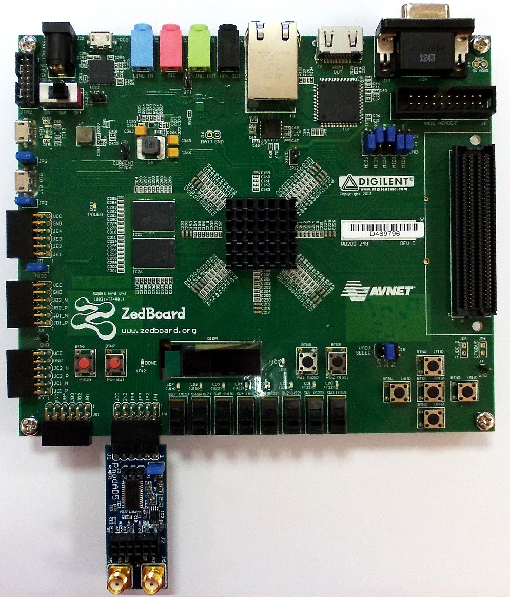
Zedboard (Digilent)
Quick Start Guide
The bit file provided in the project archive combines the FPGA bit file and the SDK elf files. It can be used for a quick check on the system. All you need is the hardware, a PC running a UART terminal, and the programmer (IMPACT).
Required Hardware
One of the supported FPGA boards listed above
PmodAD5 (Digilent)
Required Software
AMD Xilinx ISE 14.4 (Programmer (IMPACT) is sufficient for the demo and is available on Webpack)
A UART terminal (Tera Term / HyperTerminal), baud rate 115200 for the Avnet LX-9 MicroBoard and Digilent Zedboard, or 9600 for the Digilent Nexys3 Board
Board Setup
Avnet LX9 MicroBoard
Extract the project from the archive file
(AD7193_<board_name>.zip) to the location you desire.
Connect the PmodAD5 to the J5 connector of the LX9 board, pins 1 to 6. You can use an extension cable for ease of use. Connect the USB cable from the PC to the USB-UART female connector of the board for the UART terminal. The board will be programmed through its USB male connector.
Digilent Nexys3
Extract the project from the archive file
(AD7193_<board_name>.zip) to the location you desire.
Connect the PmodAD5 to the JA connector of the Nexys3 board, pins JA1 to JA6. You can use an extension cable for ease of use. Connect the USB cables from the PC to the board: one for programming (Digilent USB device) and one for the UART terminal (FT232R USB UART).
Digilent Zedboard
Connect the PmodAD5 to the JA connector of the Zedboard. You can use an extension cable for ease of use. Connect the USB cables from the PC to the board: one for programming (Digilent USB device) and one for the UART terminal (FT232R USB UART).
FPGA Configuration
Nexys3 and LX-9 MicroBoard
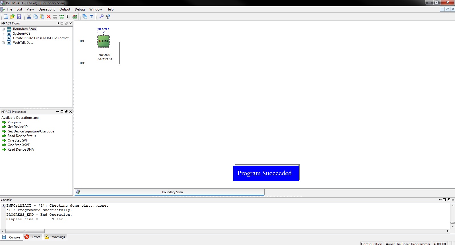
Start IMPACT and double click “Boundary Scan”.
Right click and select Initialize Chain. The program should recognize the Spartan-6 device.
Start a UART terminal (set to the appropriate baud rate).
Program the device using the bit file provided in the project archive, located in the
swfolder (ad7193/sw/AD7193.bit).
Zedboard
Run the download.bat script from the bin folder downloaded from
the project repository. The script will automatically configure the ZYNQ
SoC and download the elf file afterwards.
If the download script fails to run, modify the AMD Xilinx Tools path in
download.bat to match your AMD Xilinx installation path.
Demo Modes
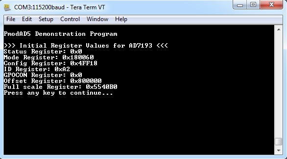
If programming was successful, messages will appear on the terminal window. After programming the AD7193, the program displays the values of all internal registers. After that, it runs through 5 demo modes:
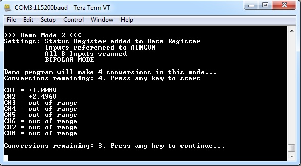
Read voltage values referenced to AINCOM, unipolar mode
Read voltage values referenced to AINCOM, bipolar mode
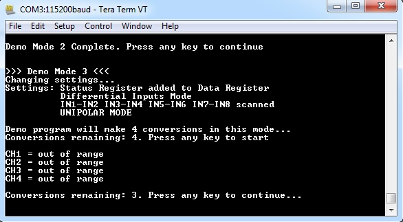
Read differential voltage values, unipolar mode
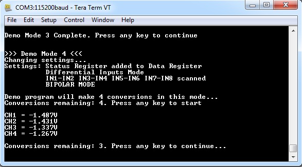
Read differential voltage values, bipolar mode
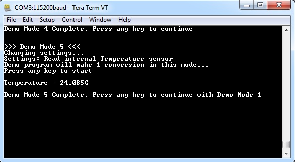
Read die temperature value

Functional Description
The reference design is a simple SPI interface, containing CS, SCLK, MISO, and mosi, plus a GPIO to read the RDY status on the MISO line. The information is displayed on UART.
The hardware SPI access allows sending and receiving data from the AD7193, programming its internal registers in order to select which channels should be converted (referenced to AINCOM or a differential pair), gain, sampling frequency, etc.
Note
Connecting the PmodAD5 to the boards using an extension cable provides ease of use.
UART must be set to 115200 baud rate for the Avnet LX-9 MicroBoard and Zedboard, or 9600 baud rate for the Digilent Nexys3 Board.
When using AVDD > DVDD (= 3.3 V), JP1 on PmodAD5 must be removed. The range for AVDD is 3.0 V to 5.25 V.
If using the AMD Xilinx SDK integrated console as a terminal client, uncomment all the commented
getchar();calls inmain.c, because the console sees Enter as two consecutive keypresses. If using Tera Term or similar software, do not modify anything.
When using the Zedboard reference design to develop your own software,
make sure that the following options are set in system_config.h:
#define USE_PS7          1
#define USE_SPI          1
#define USE_I2C          0
#define USE_TIMER        0
#define USE_EXTERNAL     0
#define USE_GPIO         0
Downloads
Avnet LX-9 MicroBoard and Digilent Nexys3 reference design source code may be available on the EVAL-AD7193ASDZ product page.
Digilent Zedboard: