User Guide
The EVAL-AD5758SDZ is a full-featured evaluation board for the AD5758, a single-channel, 16-bit, voltage and current output digital-to-analog converter (DAC) with on-chip dynamic power control (DPC), integrated fault diagnostics, and HART connectivity. The board carries an on-board 2.5 V ADR4525 reference and an ADP1031-1 isolated power management unit (PMU) with integrated SPI signal isolation.
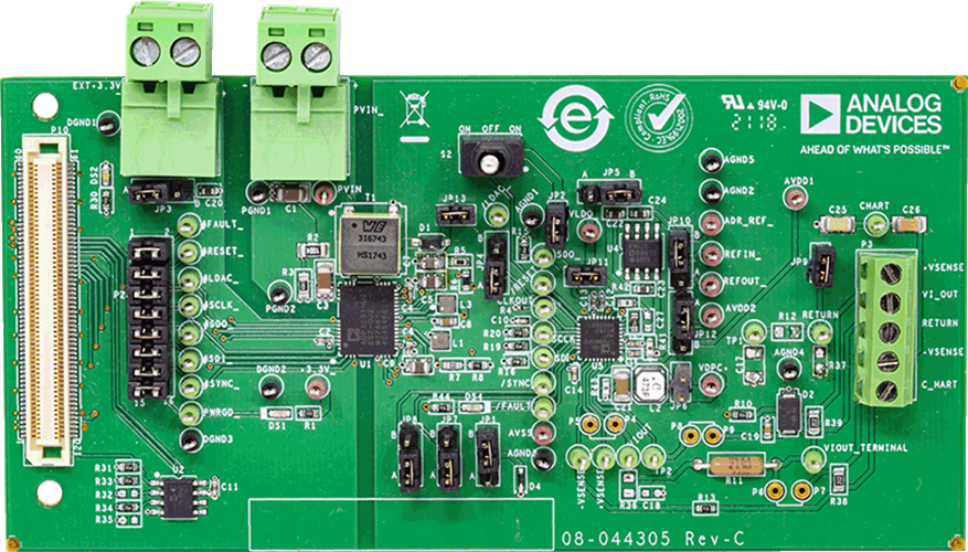
The complete hardware description of the evaluation board, including the full link/jumper option tables, schematics, and bill of materials, is documented in the EVAL-AD5758 User Guide (UG-1268). This page focuses on evaluating the board with a ZedBoard FPGA carrier using the HDL reference design and No-OS, which is the setup recommended in this documentation.
Note
The EVAL-AD5758SDZ can be evaluated in two ways:
With an FPGA carrier (ZedBoard) using the HDL reference design and Linux/no-OS software. This is the platform covered here.
With the EVAL-SDP-CS1Z (SDP-S) controller board and the ACE software on a PC, as described in UG-1268. Refer to UG-1268 for that flow.
The FPGA carrier is programmed with the AD5758 HDL reference design. For the supported carrier (ZedBoard), the required jumper settings, the block diagram, and the build instructions, refer to the AD5758-SDZ HDL reference design documentation.
Overview
The AD5758 operates with a power supply range from −33 V on AVSS to +33 V on AVDD1, with a maximum of 60 V between the two rails. Its key features include:
Single-channel, 16-bit resolution
Programmable voltage outputs (0 V to 5 V, 0 V to 10 V, ±5 V, ±10 V) and current outputs (0 mA to 20 mA, 0 mA to 24 mA, 4 mA to 24 mA, ±20 mA, ±24 mA)
On-chip dynamic power control (DPC) using a buck dc-to-dc converter to minimize package power dissipation
Integrated 12-bit diagnostic ADC and fault-protection switches
SPI interface with CRC and watchdog timer
HART signal coupling via the CHART pin
Applications include industrial process control, actuator and valve control, programmable logic controllers (PLCs), and HART network connectivity.
Hardware guide
Hardware configuration
The evaluation board ships with a set of link (jumper) options that are preconfigured to sensible defaults. For the full list of links (JP1 to JP13, P10, and S2) and their functions, see Table 1 of UG-1268.
When using the board with the ZedBoard and the HDL reference design, confirm the following default link positions:
Link |
Default |
Function |
|---|---|---|
JP1 |
B |
Selects the VOUT3 pin of the ADP1031-1 (position A selects AVSS to GND for the unipolar, current-output-only supply option). |
JP4 |
A |
Connects the LDAC pin to GND (position B connects LDAC to VLOGIC). |
JP6 |
Not inserted |
When inserted, shorts VDPC+ to AVDD1, bypassing the positive dc-to-dc circuitry. Leave open to use the on-chip DPC buck converter. |
JP7 |
A |
Connects the AD0 address pin to GND (position B connects it to VLOGIC). |
JP8 |
A |
Connects the AD1 address pin to GND (position B connects it to VLOGIC). |
JP10 |
B |
Selects the ADR4525 output as the REFIN input (position A selects the AD5758 REFOUT pin). |
JP11 |
Inserted |
Selects the 3.3 V VLDO output as the source for the VLOGIC input. |
Danger
The EVAL-AD5758SDZ can operate at high voltages (up to 60 V between the AVDD1 and AVSS rails). Take appropriate care when powering and probing the board.
Power supply
The on-board ADP1031-1 PMU generates three of the four supplies required by the AD5758 from a single bench-top input: AVDD1 (+26.7 V), AVDD2 (+5.15 V), and AVSS (−15.4 V). The fourth supply, VLOGIC (3.3 V), is provided from the AD5758 VLDO output through the JP11 link.
Apply the bench-top power supply and connector cables per UG-1268. AVDD2 requires a voltage between 5 V and 33 V; the full AVSS/AVDD1 range is −33 V to +33 V with a 60 V maximum between rails.
Serial communication and control
When the board is used with the ZedBoard, the FPGA drives the SPI interface (SCLK, SDI, SDO, SYNC) and the RESET, LDAC, and FAULT signals of the AD5758 through the EVAL-SDP-CK1Z (FMC-I-SDP) interposer and the FMC LPC connector. The P10 link and the S2 link allow the digital signals to be disconnected from the controller and driven from an external source; leave them in their default positions for standard operation.
Schematic, PCB Layout, Bill of Materials
Design support files for the EVAL-AD5758SDZ evaluation board, including schematics, PCB layout, and bill of materials, are available on the AD5758 product page. Refer to the EVAL-AD5758 User Guide (UG-1268) for the full evaluation board user guide.
Getting started
To evaluate the board with the ZedBoard:
Verify the link (jumper) settings as described in the Hardware configuration section above.
Prepare the SD card with the HDL reference design and no-OS software, as described in the quick start guide.
With the ZedBoard powered off, insert the prepared SD card, plug the EVAL-SDP-CK1Z (FMC-I-SDP) interposer into the ZedBoard FMC LPC connector, and mount the EVAL-AD5758SDZ onto the interposer.
Connect a 24 V bench-top supply to the PVIN connector, but keep the supply output turned off for now.
Power on the ZedBoard using its own power supply, then turn on the 24 V supply to the EVAL-AD5758SDZ.
Use the no-OS application to control the DAC output.
For the step-by-step carrier setup, see the ZedBoard quick start guide.