User guide
Warning
The AD-FMCJESDADC1-EBZ is a legacy product and is no longer actively supported. This documentation is provided for reference only.
Hardware guide
Specifications
The AD-FMCJESDADC1-EBZ board’s primary purpose is to easily understand, validate, and verify the JESD204B interface with various manufacturers’ FPGAs (designs available for Altera and Xilinx).
When fitting into the small FMC form factor, various tradeoffs were made that limit performance to the first Nyquist zone. These tradeoffs in size/power/performance are normally the things that Analog Devices advises customers to avoid in order to achieve maximum performance.
Clocking
The AD-FMCJESDADC1-EBZ uses the AD9517-1, a small (7.0 mm x 6.75 mm), low power (~1.4 W) multi-output clock distribution IC with subpicosecond jitter performance, along with an on-chip PLL and VCO. It is driven by a single 30.72 MHz crystal and generates the necessary clocks for the system: 2.45760 GHz, 245.760 MHz, and 30.72 MHz.
The ADIsimCLK tool provides the following data about the clocking system on the 245.760 MHz (which drives the AD9250) outputs:
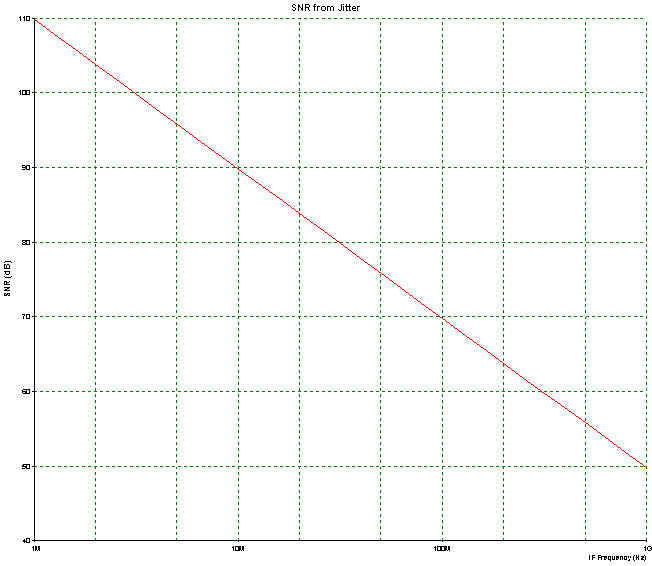
Broadband Jitter (>1kHz) = 516fs (rms)
   SNR = 69.79dB ENOB = 11.63bits
   at IF Freq = 100 MHz
Integrated Phase Noise from 100kHz to 1.25MHz
  Timing Jitter = 304fs rms
  Phase Jitter EVM = 0.05% rms
  Phase Jitter = 0.027 degrees rms
  ACI/ACR = -69.6dBc
Delay from Ref to OUT2 is 420ps
This matches up with the datasheet when using the internal VCO. To improve this number, an external VCXO could have been used (would decrease the jitter to ~54 fs rms), but this would have increased the size and violated the height requirements of the FMC specification.
Analog Front End
The AD9250 datasheet and the golden evaluation board recommend a Differential Double Balun Input Configuration (Figure 41 in the datasheet), with this note:
Important
From the AD9250 Datasheet: At input frequencies in the second Nyquist zone and above, the noise performance of most amplifiers is not adequate to achieve the true SNR performance of the AD9250. For applications where SNR is a key parameter, differential double balun coupling is the recommended input configuration (see Figure 41).
The AD-FMCJESDADC1-EBZ uses a single differential transformer (Minicircuits TC4-1W) - as shown in Figure 40 of the datasheet - due to its smaller size. The specific transformer is specified from 3 to 800 MHz, but is only linear (±0.5 dB insertion loss/input return loss) from 10 to 100 MHz, limiting operation to the first Nyquist zone before the converter sees significant losses on the input side.
This transformer was chosen as a good trade-off of size (3.8 mm x 3.8 mm x 3.8 mm), power (250 mW RF), and secondary/primary impedance ratio (4:1) suitable for the first Nyquist zone.
Software guide
Linux
Help & Support
Hint
Build an HDL project contains all the documentation, build instructions and register map tables.
Browse the HDL GitHub repository: library components and projects.
Questions? Ask on: