User guide
Evaluation boards available
Two evaluation boards are available for the AD469x family:
Board |
Form Factor |
Supported Devices |
Controller Board |
|---|---|---|---|
FMC |
AD4695, AD4696, AD4697, AD4698 |
EVAL-SDP-CH1Z (SDP-H1) |
|
Arduino Uno Shield |
AD4691, AD4692, AD4693, AD4694 |
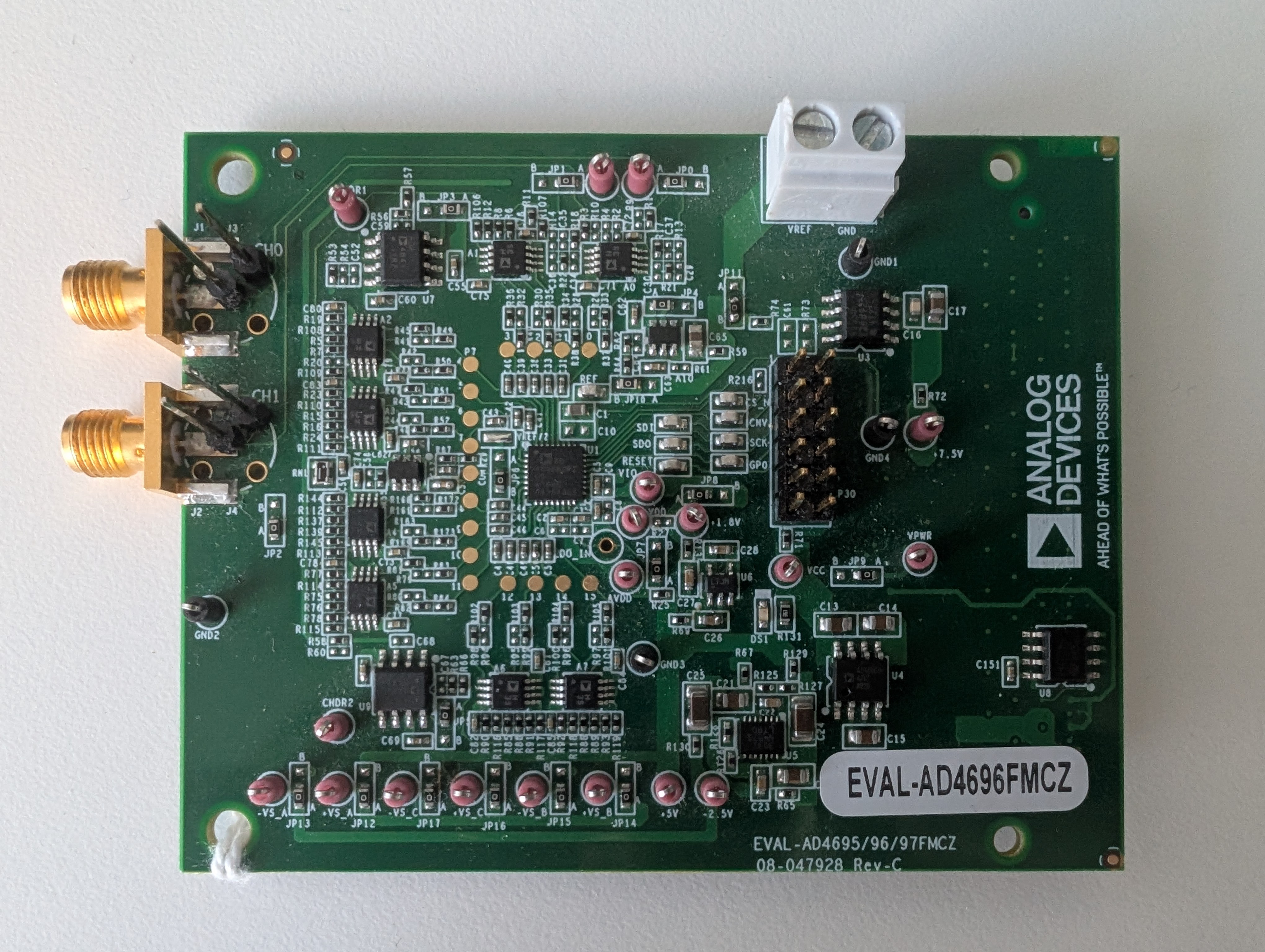
EVAL-AD4696FMCZ
The EVAL-AD4696FMCZ demonstrates the performance of the AD4696, a 16-channel, 16-bit, 1 MSPS multiplexed SAR ADC. It features two externally driven analog input channels (IN0 and IN1) for AC evaluation via SMA connectors and 14 DC channels (IN2 through IN15) with on-board bias voltages for noise and settling evaluation. The board connects to a host controller via a 160-pin FMC connector.
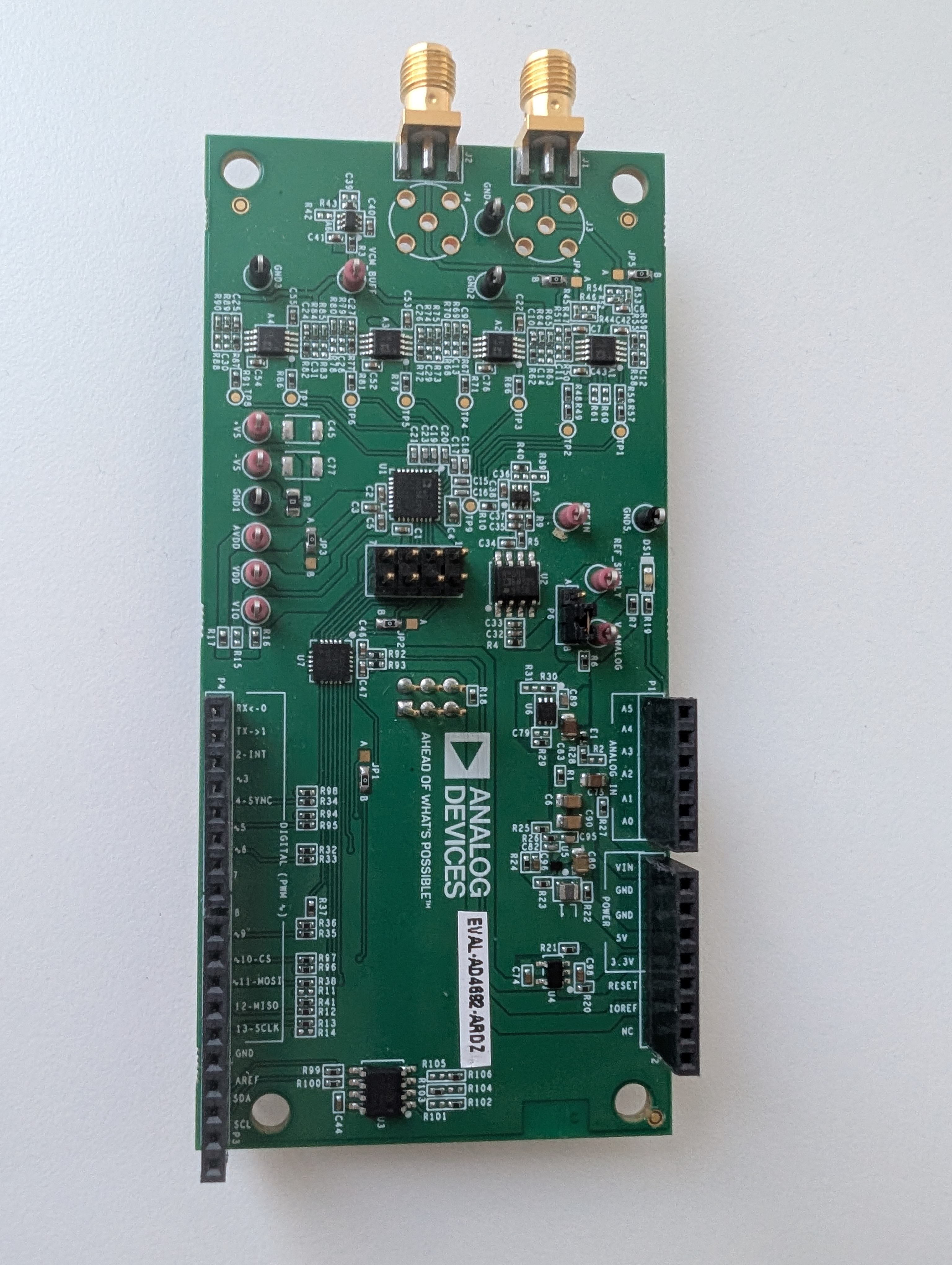
EVAL-AD4692-ARDZ
The EVAL-AD4692-ARDZ demonstrates the performance of the AD4692 family of Easy Drive multiplexed SAR ADCs with per-channel averaging filters. It features two AC input channels (CH0 and CH1) via SMA connectors and six DC channels (CH2 through CH7). The remaining eight channels are tied to ground. The board conforms to the Arduino Uno Shield standard and interfaces with the SDP-K1 controller board.
Hardware guide
Power supply
EVAL-AD4696FMCZ power supply
The EVAL-AD4696FMCZ is designed to operate from a 12 V supply (VPWR_12V) and a 3.3 V supply (VCC_HOST) provided from the host controller board via the FMC connector (P1). Alternatively, VPWR_12V can be provided from an external source via the VPWR test point.
The on-board power circuitry generates the following rails:
Rail |
Voltage |
Function |
|---|---|---|
VPWR_12V |
12 V |
Input supply via FMC connector or VPWR test point |
+7.5 V |
7.5 V |
Generated by ADP7142 from VPWR_12V; powers amplifier supply banks |
+5 V |
5 V |
Generated by LT3032 from 7.5 V; powers reference and ADC |
+1.8 V |
1.8 V |
Generated by LT1761 from 5 V; powers VIO and digital I/O |
-V_SUP |
-3.3 V |
Generated by ADM660 from VCC_HOST |
-2.5 V |
-2.5 V |
Generated by LT3032 from -V_SUP; powers amplifier negative supply banks |
The voltage rails can be powered externally by removing the 0 Ohm resistors at the outputs of the power management ICs:
Supply Rail |
Resistor |
Notes |
|---|---|---|
7.5 V |
R123 |
Disconnect from ADP7142 |
5 V |
R129 |
Disconnect from LT3032 |
1.8 V |
R135 |
Disconnect from LT1761 |
-2.5 V |
R130 |
Disconnect from LT3032 |
EVAL-AD4692-ARDZ power supply
The EVAL-AD4692-ARDZ is powered from the 5 V and 3.3 V pins on the Arduino header of the controller board.
Rail |
Voltage |
Function |
|---|---|---|
V_ANALOG |
5 V |
MAX17291 boosts the 5 V header, ADP7118 regulates to low-noise 5 V; powers AFE, reference, and ADC |
LDO_1.8V |
1.8 V |
ADP150 regulates 3.3 V header to 1.8 V; powers ADC I/O logic and VDD |
+VS |
5 V |
Positive supply for ADC driver amplifiers (derived from V_ANALOG) |
-VS |
GND |
Negative supply for ADC driver amplifiers (connected to ground by default) |
The V_ANALOG, +VS, and -VS rails can be powered externally by depopulating their associated connection resistors (R6, R7, R8) and applying signals to the corresponding test points. The AD4692 LDO_IN, VIO, and VDD pins can also be driven externally (see R17, R16, R15 respectively).
Voltage reference
EVAL-AD4696FMCZ reference
The EVAL-AD4696FMCZ includes an on-board precision 5 V reference provided by the ADR4550 (U3). The ADA4807-1 (A10) functions as a reference buffer. Jumper JP11 selects between the on-board reference (Position B, default) and an external user-supplied reference source via the P5 terminal block (Position A).
The reference source also generates a dedicated VREF/2 voltage used for the COM pin when configuring pseudo-bipolar mode.
EVAL-AD4692-ARDZ reference
The EVAL-AD4692-ARDZ includes an on-board precision 4.096 V reference provided by the ADR4540. An ADA4807-1 in unity-gain buffer configuration provides the buffered REF_BUF signal to the AD4692. The ADR4540 also generates the CHDR signal used to DC-bias the on-board input channels.
Jumper P6 selects between the on-board 5 V analog rail (Position B, default) and an external power supply (Position A) for driving the ADR4540.
Analog front end
EVAL-AD4696FMCZ analog inputs
The EVAL-AD4696FMCZ includes an ADC driver amplifier for each of the 16 analog inputs:
IN0 and IN1 (AC channels): Driven by an ADA4805-2 dual op amp (A0), configured as unity-gain buffers by default. These channels interface with precision signal generators via SMA connectors (J1/J3 for CH0, J2/J4 for CH1). The A0 amplifiers can be configured for unity-gain, non-inverting gain, or inverting topologies by modifying passive components and jumper settings (JP0, JP1).
IN2 through IN15 (DC channels): Driven by seven LT6237 dual op amps. These channels are biased to fixed DC voltages (2.5 V by default) generated on-board via resistor dividers from the CHDR signals. The DC channels are provided for evaluating noise and settling accuracy when sequencing the multiplexer.
EVAL-AD4692-ARDZ analog inputs
The EVAL-AD4692-ARDZ includes ADA4807-2 dual op amps as ADC drivers, configured as unity-gain buffers by default:
CH0 and CH1 (AC channels): Receive input signals via SMA connectors. A DC offset (CHDR) is applied through a summing junction to support bipolar and floating output signal generators. These channels can be configured for unity-gain, non-inverting gain, inverting, low-pass filter, or bypass topologies.
CH2 through CH7 (DC channels): Biased by the CHDR signal through resistor dividers (default: two 10 kOhm resistors, resulting in CHDR/2 at the non-inverting input). These channels evaluate settling accuracy when sequencing the multiplexer.
CH8 through CH15: Tied to ground.
Digital interface
EVAL-AD4696FMCZ digital interface
The EVAL-AD4696FMCZ provides access to the AD4696 digital interface pins via a 160-pin FMC connector (P1) and a 12-pin PMOD header (P30). The SPI signals (CS, SDI, SDO, SCK) and control signals (CNV, RESET, BSY_ALT_GP0) are routed through both connectors. VIO is set to 1.8 V by default via the on-board LT1761 (JP8 Position A). Jumper JP31 connects CS and CNV for 4-wire SPI operation.
EVAL-AD4692-ARDZ digital interface
The EVAL-AD4692-ARDZ uses SPI protocol via the Arduino Uno digital headers (P3 and P4). An ADG3308 bidirectional logic level translator converts between the 1.8 V logic level of the AD4692 and the 3.3 V logic level of the controller board. The board also includes an EEPROM for board identification.
Hardware configuration
EVAL-AD4696FMCZ link configuration
EVAL-AD4692-ARDZ configuration
Software guide
The evaluation board is supported both with Linux (using the Libiio library) and with no-OS (bare metal). The Libiio library is cross-platform (Windows, Linux, Mac) with language bindings for C, C#, Python, and others. Applications that can be used with it are:
Python support is available through the pyadi-iio library.
Drivers
The driver source code is available at:
Board |
Firmware |
Source code |
Documentation |
|---|---|---|---|
EVAL-AD4696FMCZ |
Linux |
||
EVAL-AD4696FMCZ |
no-OS |
- |
|
EVAL-AD4692-ARDZ |
Linux |
- |
The Linux driver is always exposed via the Linux Industrial I/O Subsystem. To get started with Linux drivers, see the Kernel and devicetrees page, and for no-OS drivers, checkout no-OS drivers guide.
HDL design
The AD469x HDL reference design documentation can be found at AD469X-EVB HDL project.
No-OS project
The no-OS example project can be found at projects/ad469x_evb.
Troubleshooting
A troubleshooting guide for common issues with ADI evaluation systems can be found at Troubleshooting.