EVAL-AD4130-8WARDZ Hardware Guide
Set-up Procedures
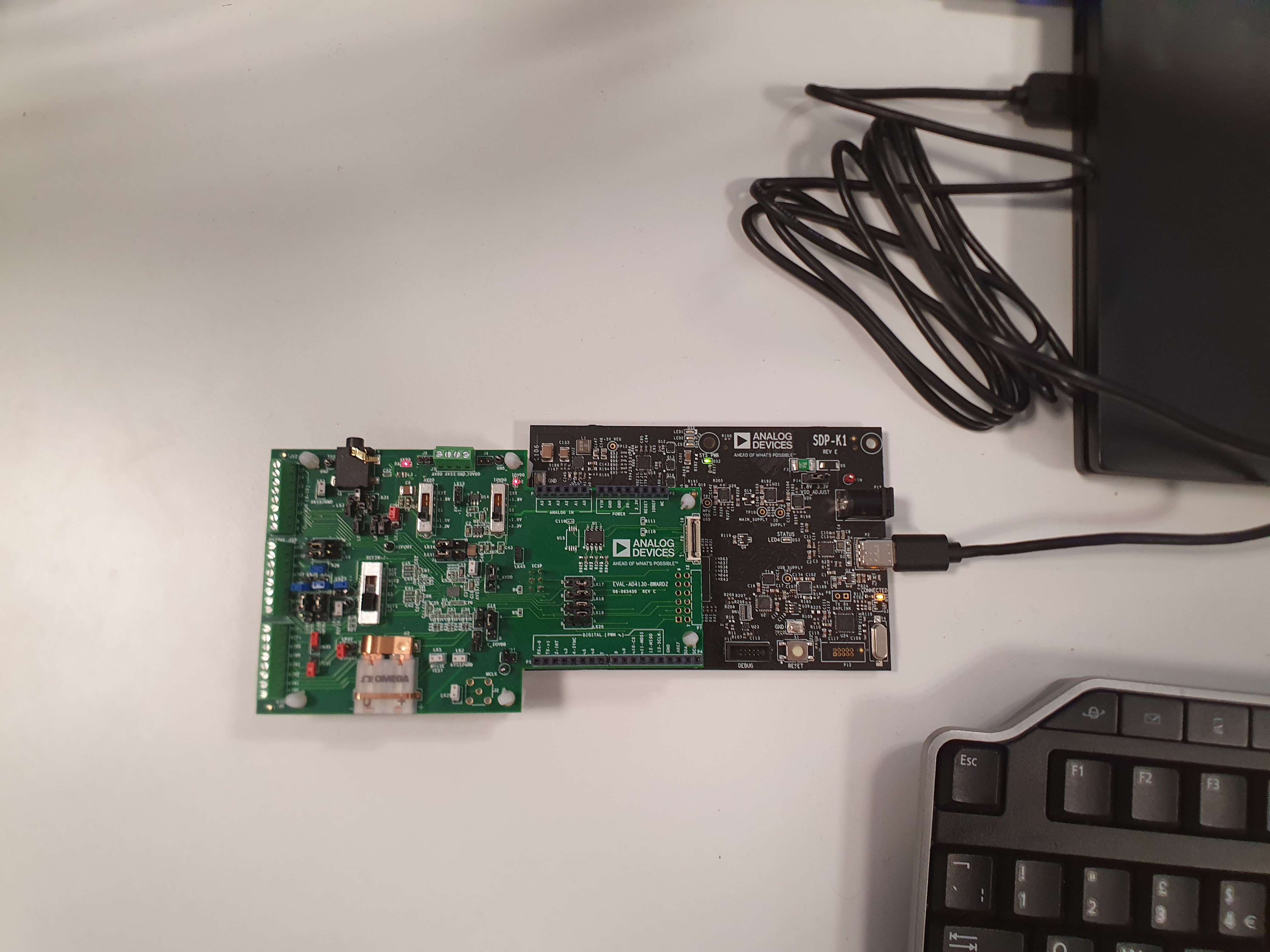
After following the instructions in the Software Procedures section, set up the evaluation and SDP-K1 board as detailed in this section.
Warning
The evaluation software and drivers must be installed before connecting the EVAL-AD4130-8WARDZ evaluation board and EVAL-SDP-CK1Z board to the USB port of the PC to ensure the PC correctly recognizes the evaluation system.
Connect the EVAL-AD4130-8WARDZ to the controller board
Using the Arduino Connectors
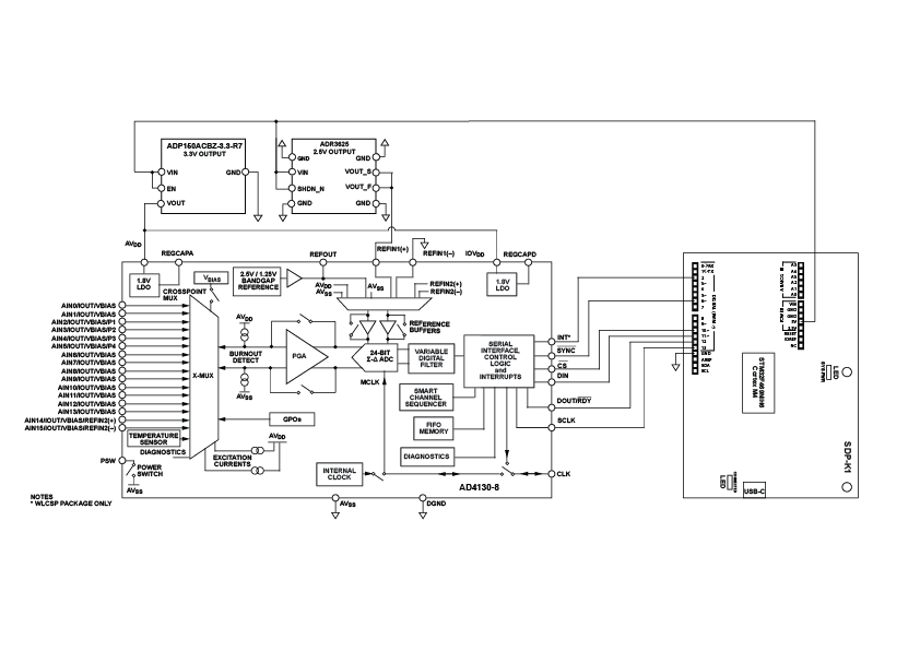
Block Diagram
Hardware Link Options
Link Numbers |
Colour |
Default Position |
Description |
Rough Board Location |
|---|---|---|---|---|
LK1-3 |
White |
Inserted |
Ties AVSS and DGND together |
N/A |
LK4 |
Black |
A |
External Reference voltage select: Pos A: REFIN + is connected to the external +2.5V reference. Pos B: REFIN + is connected to the external +1.8V reference (+1.8V reference not currently available on the board). |
Right of J10 |
LK5 |
Blue |
Inserted |
Noise Test. Channels AIN0 + AIN1 |
Right of Thermocouple Connection (A2) |
LK6 |
White |
Inserted |
REFIN(-) to AVSS |
Left of Switch S3 |
LK7 |
Black |
A |
External +2.5V Reference: Pos A: ADR391B Pos B: ADR3625B (The ADR3625B is not currently available on the board) |
Right of J10 |
LK8 |
Black |
Uninserted |
Connects AIN10 to R95. When used with LK9 you can use the AD4130-8 to measure it’s own IOVDD current |
Left of T_IOVDD |
LK9 |
Black |
Uninserted |
Connects AIN11 to R95. When used with LK8 you can use the AD4130-8 to measure it’s own IOVDD current |
Left of T_IOVDD |
LK10 |
Black |
Uninserted |
Connects AIN12 to R96. When used with LK11 you can use the AD4130-8 to measure it’s own AVDD current |
Left of Switch S1 |
LK11 |
Black |
Uninserted |
Connects AIN13 to R96. When used with LK10 you can use the AD4130-8 to measure it’s own AVDD current |
Left of Switch S1 |
LK12 |
White |
Uninserted |
Connects AVSS to -1.8V. LK1-3 must be removed before this jumper is inserted |
Right of Switch S1 |
LK14 |
Black |
Uninserted |
Connects REFIN(+) to AVDD |
Below 3.5mm Jack Connection (A1) |
LK15 |
Black |
A |
ADP150-3.3 Powered up: Pos A: LDO is on Pos B: LDO is off |
Below Switch S1 |
LK16 |
Black |
A |
ADP150-1.8 Powered up: Pos A: LDO is on Pos B: LDO is off |
Below Switch S1 |
LK17 |
Black |
A |
Arduino communication: Pos A: Standard Pos B: Alternative |
Between Arduino Connectors |
LK18 |
Black |
A |
Arduino communication: Pos A: Standard Pos B: Alternative |
Between Arduino Connectors |
LK19 |
Black |
A |
Arduino communication: Pos A: Standard Pos B: Alternative |
Between Arduino Connectors |
LK20 |
Black |
A |
Arduino communication: Pos A: Standard Pos B: Alternative |
Between Arduino Connectors |
LK21 |
Black |
Uninserted |
Connects the CLK pin to the INT pin |
Below T_IOVDD |
LK22 |
Red |
Uninserted |
Thermocouple - Cold Junction Resistor Bypass |
Left of Thermocouple Connection (A2) |
LK23 |
Blue |
Uninserted |
Short EXC+/PSW: Pos Inserted = 4 Wire Bridge |
Left of Switch S3 |
LK24 |
Blue |
Uninserted |
Short EXC+/PSW: Pos Inserted = 4 Wire Bridge |
Left of Switch S3 |
LK25 |
Blue |
Uninserted |
Short EXC+/REFIN+: Pos Inserted = 4 Wire Bridge |
Left of Switch S3 |
LK26 |
Blue |
Uninserted |
Allows the user to use an external excitation source |
Left of Switch S3 |
LK27 |
Black |
B |
REFIN(+) to connector: Pos A: To Connector J10 (BRIDGE) Pos B: To Connector J8 (RTD) |
Bottom right of J10 |
LK28 |
Black |
B |
REFIN(-) to connector: Pos A: To Connector J10 (BRIDGE) Pos B: To Connector J8 (RTD) |
Bottom right of J10 |
LK29 |
White |
Inserted |
Connects CLK pin to GND |
Left of J2 |
LK30 |
Black |
Uninserted |
Connects AIN11 to LA_ELECTORDE trace of the A1 connector |
Below 3.5mm Jack Connection (A1) |
LK31 |
Black |
Uninserted |
Connects AIN14 to RA_ELECTORDE trace of the A1 connector |
Below 3.5mm Jack Connection (A1) |
LK32 |
Black |
Uninserted |
Connects AIN15 to DRIVEN_ELECTORDE trace of the A1 connector |
Below 3.5mm Jack Connection (A1) |
LK35 |
Red |
Uninserted |
Precision Reference 5.11k ohm Resistor Bypass |
Right of J8 |
LK36 |
Red |
Uninserted |
Headroom Resistor Bypass |
Right J8 |
LK37 |
Red |
Uninserted |
Precision Sense 10k ohm Resistor Bypass |
Right of J8 |
LK45 |
Black |
Uninserted |
AVDD/IOVDD short |
Bottom Right of Switch S2 |
T_AVDD |
Black |
A |
AVDD Supply: Pos A: Directly to supply rail Pos B: Through R96 (LK10 and 11 must be inserted) which allows the AD4130-8 to measure it’s own AVDD current consumption |
Below Switch S2 |
T_IOVDD |
Black |
A |
IOVDD Supply: Pos A: Directly to supply rail Pos B: Through R95 (LK8 and 9 must be inserted) which allows the AD4130-8 to measure it’s own IOVDD current consumption |
Below Switch S2 |
S1 |
Switch |
+3.3V |
AVDD Voltage connection: Pos A: +3.3V from the LDO Pos B: +1.8V from the LDO Pos C: +1.8V from the LDO Pos D: External voltage from J7 terminal block |
Top of the Board |
S2 |
Switch |
+3.3V |
IOVDD Voltage connection: Pos A: +3.3V from the LDO Pos B: +1.8V from the LDO Pos C: +1.8V from the LDO Pos D: External voltage from J7 terminal block |
Top of the board |
S3 |
Switch |
REF1+/- |
REFIN+/- connection: Pos A: REFIN1+/- Pos B: REFIN2+/- (AIN14 and AIN15) Pos C: REFOUT and AVSS (Internal Reference needs to be enabled in the ADC Control register) |
Middle of the board |
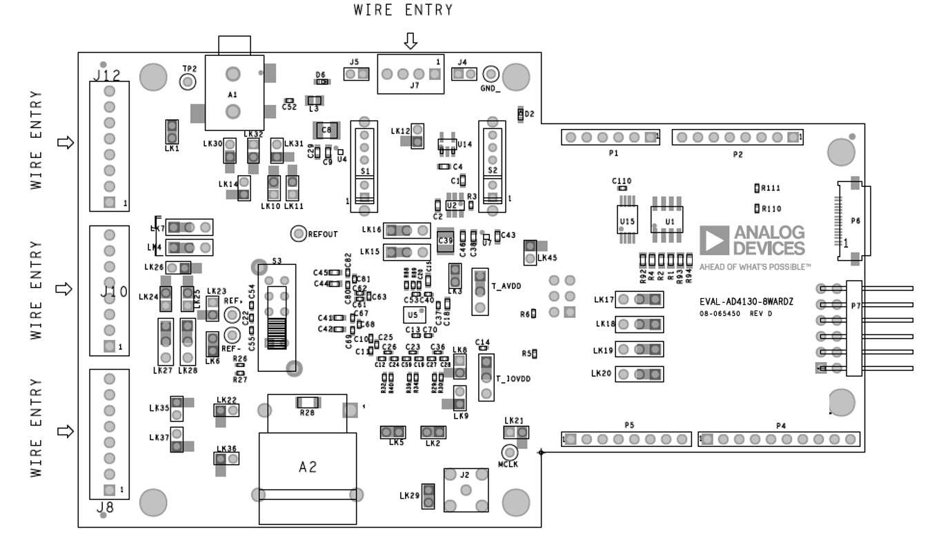
On Board Connections
3.5mm Jack Connector A1
Functionality:
ECG
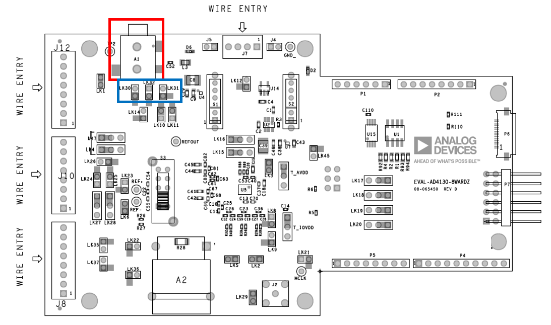
Thermocouple Connector A2
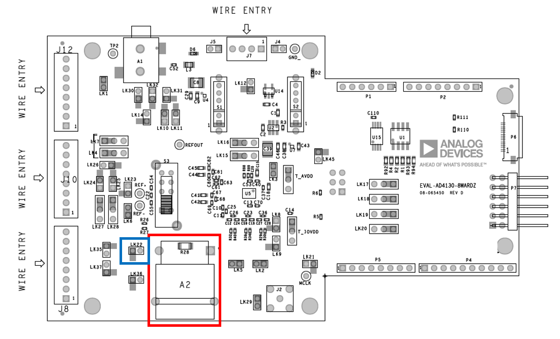
Connector J8: DC (Analog Input)
Functionality:
Noise Test
RTD
Thermocouple
Thermistor
Connection |
Function |
|---|---|
1 |
AIN0 (AINP) with DC filtering(DNI) and noise test channel. IOUT0 Excitation current for RTDs |
2 |
AIN1 (AINN) with DC filtering(DNI) and noise test channel. IOUT1 Excitation current for 3 wire RTD |
3 |
AIN 2 with DC filtering (RTD+ connection) (TC+ connection) |
4 |
AIN 3 with DC filtering (RTD- connection) (TC- connection) |
5 |
AIN 4 with DC filtering (Cold Junction+ connection) (Thermistor+ connection) |
6 |
AIN 5 with DC filtering (Cold Junction- connection) (Thermistor- connection) |
7 |
External Reference + |
8 |
External Reference - |
Connector J10: Wire Bridge (Analog Input)
Functionality:
4/6 Wire bridge
Connection |
Function |
|---|---|
1 |
Ground/shield connection |
2 |
Excitation- /Power Switch Function for Wire Bridge |
3 |
External Reference- / Sense- |
4 |
AIN 6 (AINN) with DC filtering |
5 |
AIN 7 (AINP) with DC filtering |
6 |
External Reference+ / Sense+ |
7 |
Excitation+ /AVDD supply for Wire Bridge |
8 |
Ground/shield connection |
Connector J12: DC (Analog Input)
Functionality:
DC connections for AIN8 to AIN15
Connection |
Function |
|---|---|
1 |
AIN 8 without DC filtering |
2 |
AIN 9 without DC filtering |
3 |
AIN 10 without DC filtering |
4 |
AIN 11 without DC filtering |
5 |
AIN 12 without DC filtering |
6 |
AIN 13 without DC filtering |
7 |
AIN 14 without DC filtering |
8 |
AIN 15 without DC filtering |
Connector J7: External Power
Connection |
Function |
|---|---|
1 |
External IOVDD connection |
2 |
External GND connection |
3 |
External AVSS connection |
4 |
External AVDD connection |
Digital Connectors
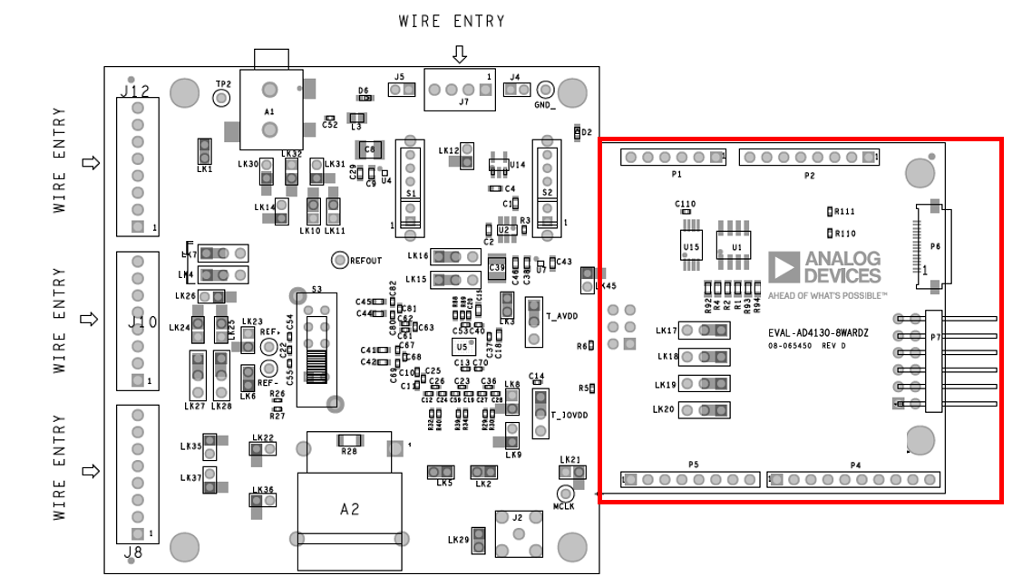
Arduino Connector P1-P5
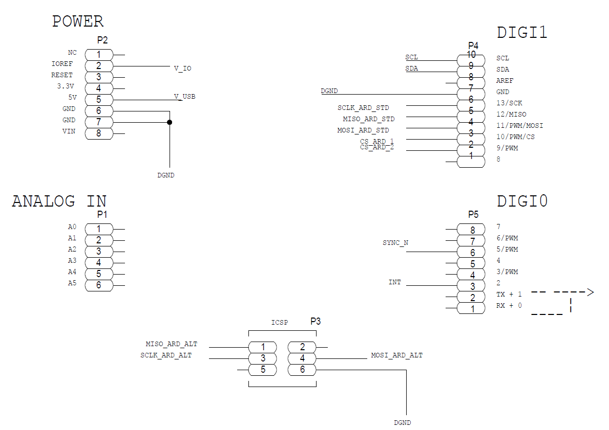
PMOD Connector P7
Connection |
Function |
Connection |
Function |
|---|---|---|---|
1 |
CS_N |
7 |
SYNC_N |
2 |
MOSI/DIN |
8 |
INT |
3 |
MISO/DOUT |
9 |
N/C |
4 |
SCLK |
10 |
N/C |
5 |
GND |
11 |
GND |
6 |
V_USB |
12 |
V_USB |
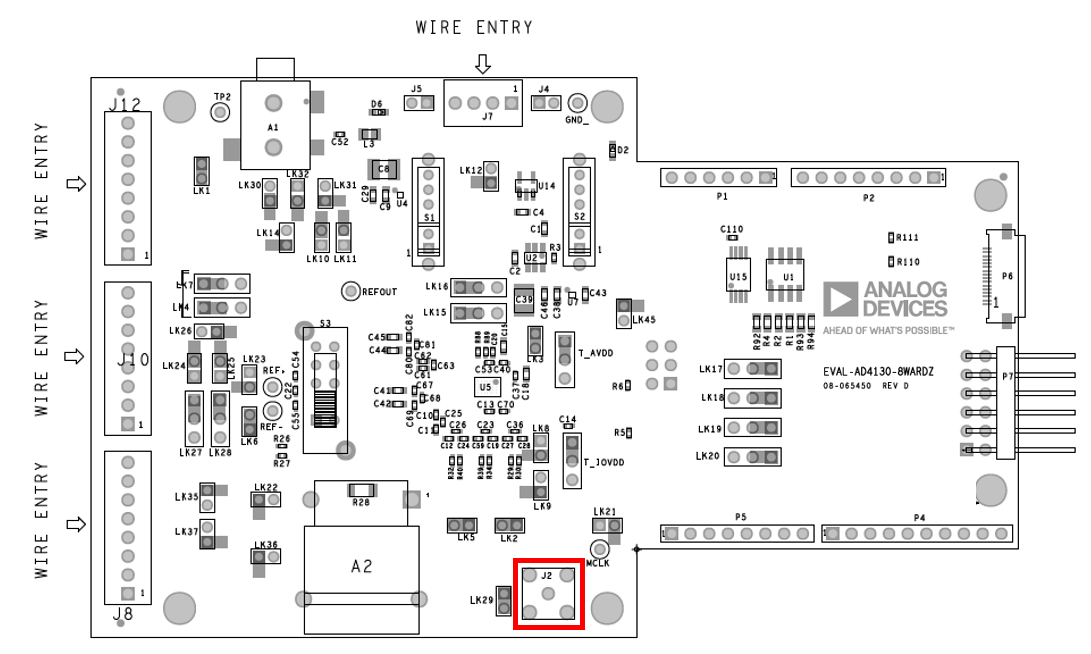
SMA/SMB Connections
There is 1 SMA/SMB connections on the board. To allow clock signals into the board.
SMB J2 Brings external MCLK to the AD4130-8
Power Supplies
The evaluation board receives power through the controller board when connected to the PC via USB. Linear regulators generate the required power supply levels from the applied USB voltage.
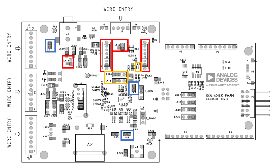
Location of AVDD, AVSS and IOVDD control links are highlighted in Red in the diagram below
Each regulators can be shut down using their shut down links highlighted in orange below
AVDD (S1) and AVSS (LK12) selection
3.3V supply (DEFAULT)
3.3V regulator supplies AVDD
AVSS tied to GND [LK1-3 (Blue)]
1.8V supply
1.8V regulator supplies AVDD
AVSS tied to GND [LK1-3 (Blue)]
±1.8V split supply
1.8 regulator supplies AVDD
-3 regulator to a -1.8V regulator supplied AVSS
VREF supply
The external reference supplies AVDD [LK14]
AVSS tied to GND [LK1-3 (Blue)]
External AVDD/AVSS
Connections on Connector J7
Supply |
Regulator |
Shut down Link (ORANGE) |
|---|---|---|
3.3V regulator |
LK15 |
|
1.8V regulator |
LK16 |
|
-3V regulator |
R3 |
|
-1.8V regulator |
R3 |
IOVDD (S2) selection
3.3V supply (DEFAULT)
3.3V regulator supplies IOVDD
GND tied to AVSS [LK1-3 (Blue)]
1.8V supply
1.8V regulator supplies IOVDD
GND tied to AVSS [LK1-3 (Blue)]
±1.8V split supply
1.8 regulator supplies AVDD
GND Split from AVSS [LK1-3 (Blue)]
Tied to AVDD (LK45)
AVDD supplies IOVDD
GND tied to AVSS [LK1-3 (Blue)]
External IOVDD/GND
Connections on Connector J7
Supply |
Regulator |
Shut down Link (ORANGE) |
|---|---|---|
3.3V regulator |
LK15 |
|
1.8V regulator |
LK16 |
Serial Interface
There are four primary signals: CS, SCLK, MOSI/DIN, and MISO/DOUT (all are inputs, except for MISO/DOUT, which is an output).
Serial communication options
Arduino connection using the SDP-K1
PMOD connector
Standalone mode
Removing the links LK17, 18, 19, 20 and using the pins from these links can then be used to fly-wire the signals to an alternative digital capture setup
Reference Options
AD4130-8 Internal Reference +2.5V/+1.25V
DEFAULT ADR391 On Board external reference
External Reference Connector J8
Option to use 5.11k ohm precision resistor (R91) insert LK35 (Used for RTD Demo mode)
Option to use 10k ohm precision resistor (R91) insert LK37 (Used for Thermistor Demo mode)
External Reference Connector J10
Selecting the reference source:
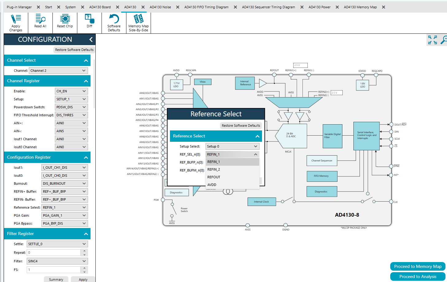
Software
Example shows setting reference for Channel 0, for channel n, go to register CONFIG[n]
Board should be correctly connected to ACE
Open AD4130-8 memory map
Search for the CONFIG[0] register
Set the REF_SEL_N[0] to the desired reference source or the Data(hex) to the relevant bits
Dedicated reference pins REFIN1 +/- (Hex value 00, Binary Value 00).
From GPIO0/1 REFIN2 +/- (Hex value 01, Binary Value 01).
Internal Reference REFIN_REFOUT (Hex Value 02, Binary Value 10).
AVDD to AVSS (Hex Value 02, Binary Value 11).
Hardware
Link Numbers |
Type |
Default Position |
Description |
Rough Board Location |
|---|---|---|---|---|
S3 |
Switch |
REF1+/- |
REFIN+/- connection: Pos A: REFIN1+/- Pos B: REFIN2+/- (AIN14 and AIN15) Pos C: REFOUT and AVSS (Internal Reference needs to be enabled in the ADC Control register) |
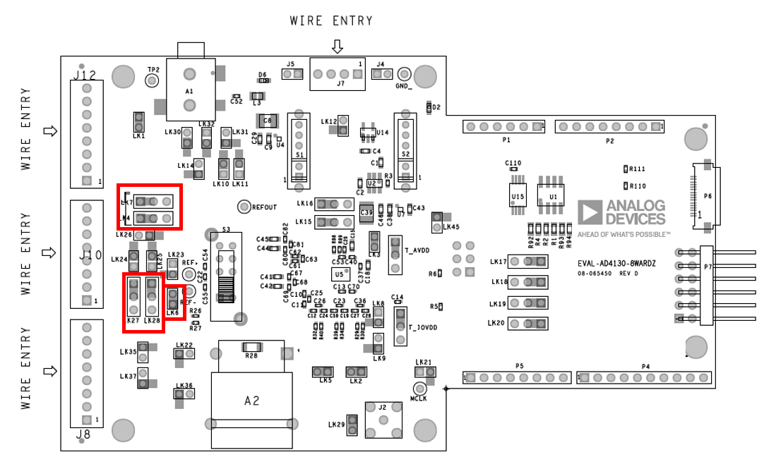
If REFIN1+/- or REFIN2+/- is selected the options below are available using links shown in the diagram below
ADR391, REFIN - shorted to AVSS (LK6)
External Reference Connector J8
External Reference Connector J10
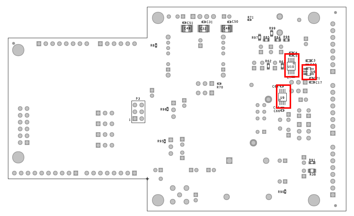
Silk Screen
Design and Integration Files
Schematics, layout files, and bill of materials are available on the EVAL-AD4130-8WARDZ product page.