Evaluating the AD9265 Analog-to-Digital Converter
Warning
Support for the AD9265-FMC with the SDP-H1 board was discontinued starting with the 2022_R2 Kuiper Linux release and will not be supported in future releases. The last release with pre-built files is 2021_R2. See all Kuiper releases.
This page describes how to evaluate the AD9265-FMC-125EBZ using the EVAL-SDP-CH1Z (SDP-H1) High Speed Controller Board, together with the VisualAnalog® and SPI Controller software. The evaluation board provides all of the support circuitry required to operate the AD9265 in its various modes and configurations.
For additional information, consult the AD9265 data sheet and the UG-074 User Guide.
Typical Measurement Setup
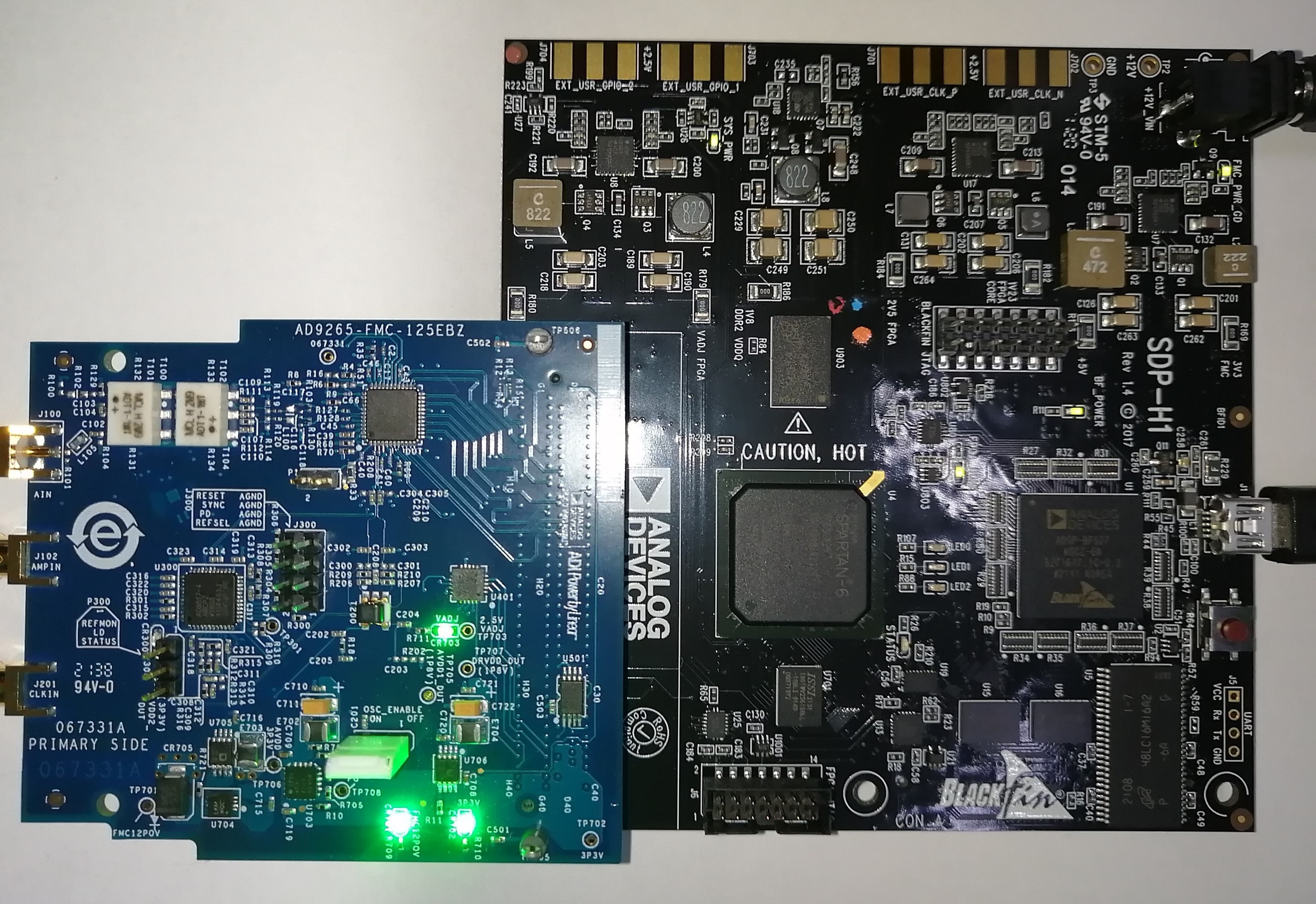
Features
Helpful Documents
AD9265 data sheet
EVAL-SDP-CH1Z, SDP-H1 High Speed Controller Board for System Development Platform
AN-905 Application Note, VisualAnalog Converter Evaluation Tool Version 1.0 User Manual
AN-878 Application Note, High Speed ADC SPI Control Software
AN-877 Application Note, Interfacing to High Speed ADCs via SPI
AN-835 Application Note, Understanding ADC Testing and Evaluation
UG-074 User Guide, User Guide for FIFO5 AD9265 Evaluation Board
Software Needed
Equipment Needed
Analog signal source (preferably SMA 100A Signal Generator)
Antialiasing filter
Sample clock source (if not using the on-board oscillator)
12 V power supply
1-meter SMA cable
PC running Windows®
USB-Mini-B cable
AD9265-FMC-125EBZ board
EVAL-SDP-CH1Z System Development Platform Kit
Getting Started
Configuring the Board
Before using the software for testing, configure the evaluation board as follows:
Connect the evaluation board to the data capture board.
Connect one 12 V switching power supply to the EVAL-SDP-CH1Z SDP-H1 board.
Connect the EVAL-SDP-CH1Z SDP-H1 board to the PC with a USB cable (connect to J1).
When using the on-board clock, connect Pin 1 and Pin 3 of P2.
On the ADC evaluation board, use a clean, low-phase-noise signal generator to provide an input signal to the input channel (J100). Use a 1 m, shielded, RG-58, 50 Ω coaxial cable. For best results, use a narrow-band band-pass filter with 50 Ω terminations and an appropriate center frequency.
If using an external clock signal, remove the connector from P2 and connect a clean signal generator to J201.
Using the Software for Testing
Setting Up the ADC Data Capture
After configuring the board, set up the ADC data capture using the following steps:
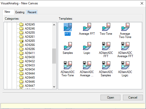
Start VisualAnalog.

Select AD9265 and double-click FFT.
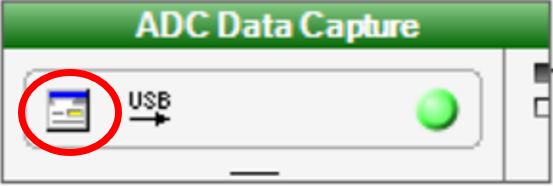
Click Settings under the ADC Data Capture section.
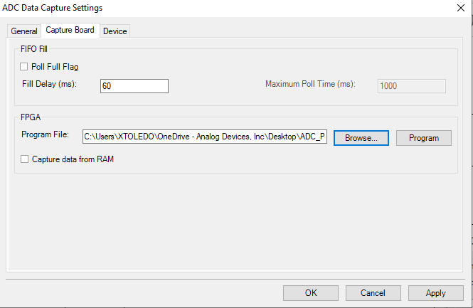
Set the device to AD9265.
Navigate to Capture Board and browse to the FPGA image file
ad9265_sdph1.bin.Click Program and verify that LED0 on the SDP-H1 illuminates. Then click OK.
Evaluation and Test
Setting Up the SPI Controller Software
Start SPI Controller.

If a “Read Test Failure” message appears, click Ignore.
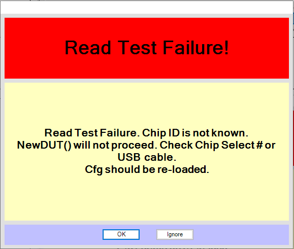
Click File > Cfg Open, find the file
ad9265_16bit_125MSspiR03.cfg, and double-click it.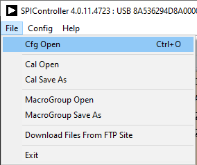
If a “Read Test Failure” message appears again, click Ignore.
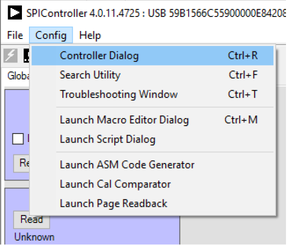
Click Config > Controller Dialog.
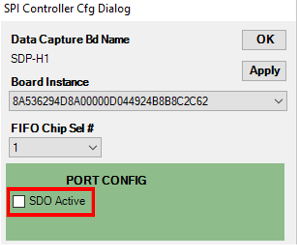
Clear the SDO Active checkbox and click OK.
Click Read Chip ID and Read Chip Grade.
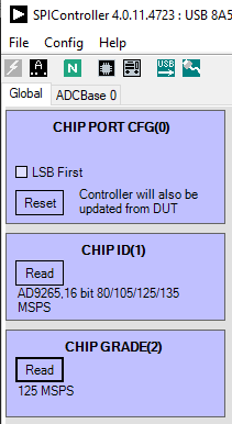
Return to VisualAnalog and click the Play button.
Adjusting the Amplitude of the Input Signal
Adjust the amplitude of the input signal so that the fundamental is at −1.0 dBFS. Verify the Fund Power reading in the left panel of the VisualAnalog Graph - AD9265 Average FFT window.
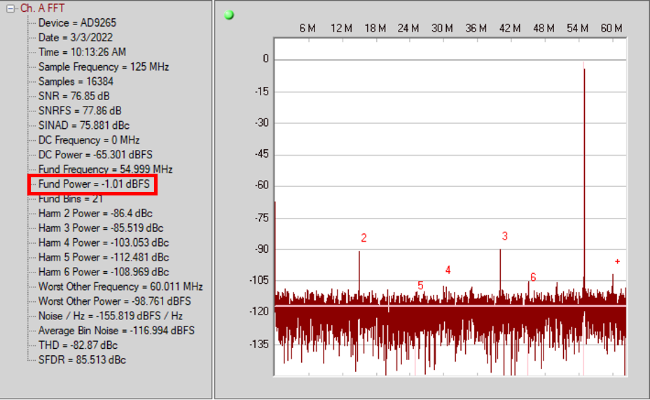
Click the disk icon in the Graph window to save the performance plot data as a
.csvfile.
When testing additional AD9265 boards, power down the EVAL-SDP-CH1Z SDP-H1 board first before swapping evaluation boards.
Troubleshooting
FFT plot appears abnormal:
If the noise floor looks normal when the signal generator is disconnected, the ADC may be overdriven — reduce the input level.
In VisualAnalog, click Settings in the Input Formatter block and verify that Number Format is set to the correct encoding (offset binary by default).
FFT appears normal but performance is poor:
Ensure an appropriate band-pass filter is used on the analog input.
Use low-phase-noise signal generators for both the clock and the analog input.
If non-coherent sampling is used, change the analog input frequency slightly, or switch to coherent frequencies.
Verify that the SPI configuration file matches the product being evaluated.
Check for mechanical stress or torque on the clock and analog input connectors.
FFT window remains blank after Run is clicked:
Confirm the evaluation board is securely connected to the EVAL-SDP-CH1Z SDP-H1 board.
Verify the FPGA has been programmed by checking that the FPGA_DONE LED is illuminated on the SDP-H1. If not, reprogram via VisualAnalog. If the LED still does not illuminate, disconnect USB and power for 15 seconds, reconnect, and repeat the SDP-H1 setup process.
Confirm the correct FPGA
.binfile was used.In the ADC Data Capture block in VisualAnalog, click Settings and verify that Clock Frequency is set correctly.
Ensure the ADC has a valid clock input.