Quickstart
The Quick Start Guide provides step by step instructions detailing how to plug in, and set up the AD-FREQCVT1-EBZ board. The ZC706 and AD-FMCOMMS3-EBZ platforms will be used to demonstrate the appropriate board and cable connections.
Supported carriers
IO layout
Carrier |
PMOD connector pin |
SPI interface |
FPGA pin name |
|---|---|---|---|
ZC706 |
PMOD1_0 |
CSN_TX |
AJ21 |
PMOD1_4 |
CSN_RX |
Y20 |
|
PMOD1_3 |
SCLK |
AB16 |
|
PMOD1_1 |
DATA |
AK21 |
|
ZC702 |
PMOD1_0 |
CSN_TX |
E15 |
PL_PJTAG_TDI |
CSN_RX |
V8 |
|
PMOD1_3 |
SCLK |
W5 |
|
PMOD1_1 |
DATA |
D15 |
|
Zed |
JA1 |
CSN_TX |
Y11 |
JA7 |
CSN_RX |
AB11 |
|
JA4 |
SCLK |
AA9 |
|
JA2 |
DATA |
AA11 |
Connecting to FMCOMMS3/4 and Cable Orienation
The AD-FREQCVT1-EBZ has four SMA connectors (TX_IN, RX_OUT, TX_OUT, RX_IN). 2 male to male SMA connectors are required to connect the AD-FREQCVT1-EBZ board to the AD-FMCOMMS3-EBZ platform.
Power is brought to the AD-FREQCVT1-EBZ board through a 3 pin cable. The connection is made at P1, which sits directly between TX_IN and RX_OUT. The power originates from the AD-FMCOMMS3-EBZ board, connector P301. It is very important to properly plug in this cable on both ends, according to the image below.
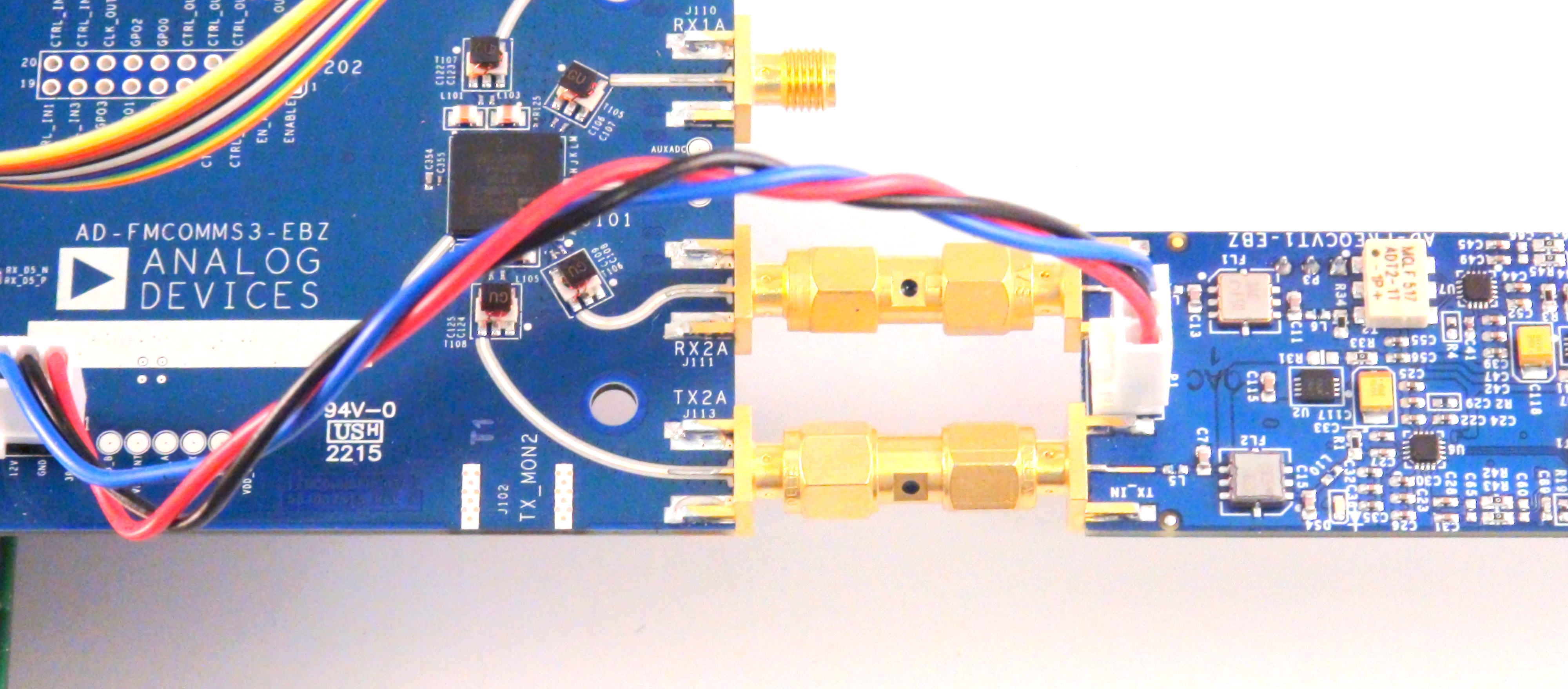
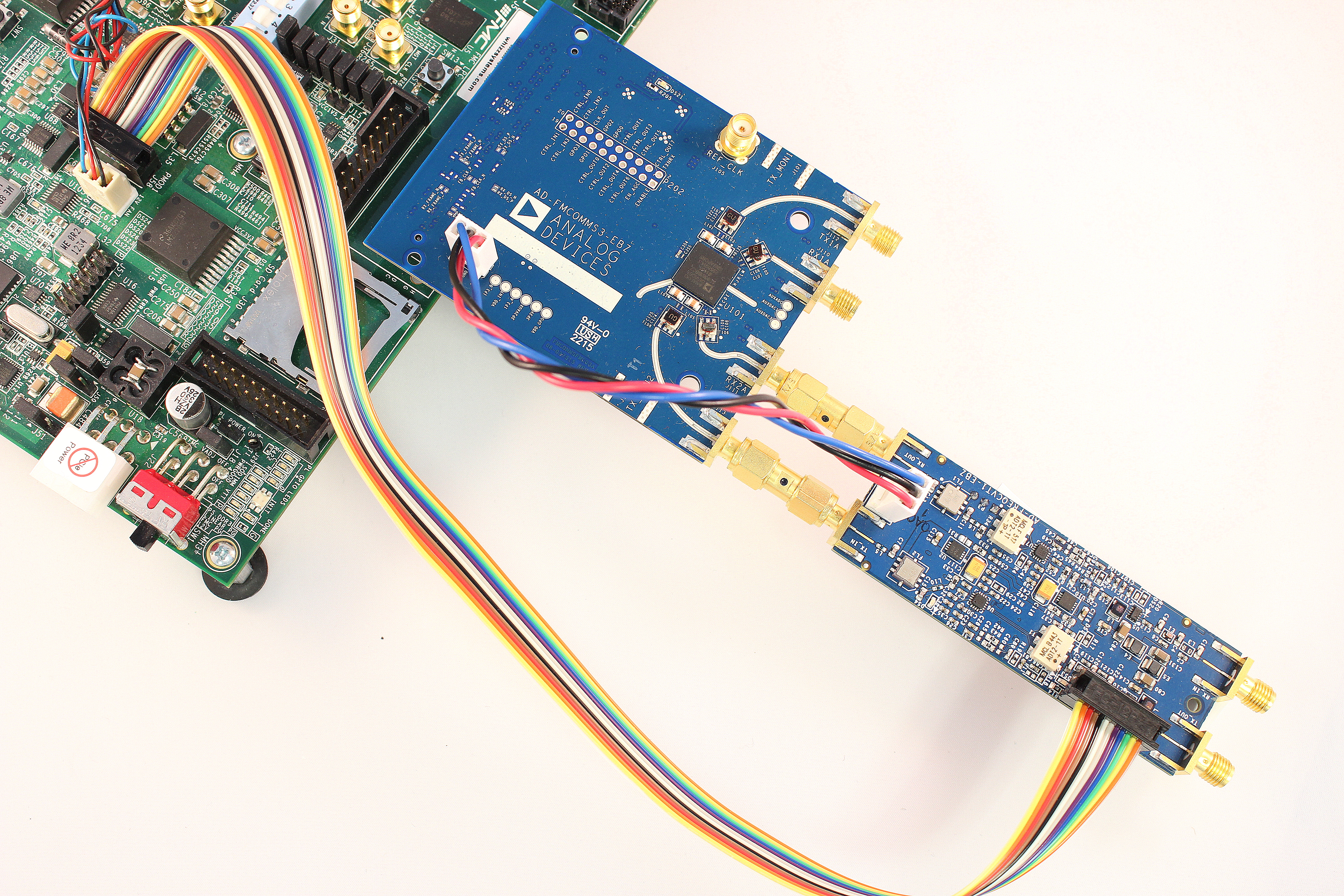
The ZC706 board provides digital controls to the AD-FREQCVT1-EBZ board through a 12-pin ribbon cable. Be careful to properly plug in both ends of the cable according to the above image. These implement a SPI protocol used for configuration, and some general purpose IO’s.
The FMCOMMS2/3 HDL design fully supports the AD-FREQCVT1-EBZ board by enabling the second SPI interface of the Processing System 7 IP core, in this way providing full access for the software to configure and setup the frequency converter board.
To use the first channel of the FMCOMMS3, line up FREQCVT1 connectors RX_OUT and TX_IN with FMCOMMS3 connectors RX1A and TX1A. This requires flipping the board upside down.
To use the second channel of the FMCOMMS3, line up FREQCVT1 connectors RX_OUT and TX_IN with FMCOMMS3 connectors TX2A and RX2A.
Software
Two ADF4351 driver instances control the external synthesizers. The OSC FMCOMMS2/3/4 plugin implement the external and internal LO synthesizer tuning logic. In case the external synthesizers are probed for presence. An additional checkbox in the plugin is displayed, allowing the user to enable or disable the tuning logic. Once enabled the RX/TX LO Spin-Button switches it’s range from 70MHz-6GHz to 1MHz-100MHz.
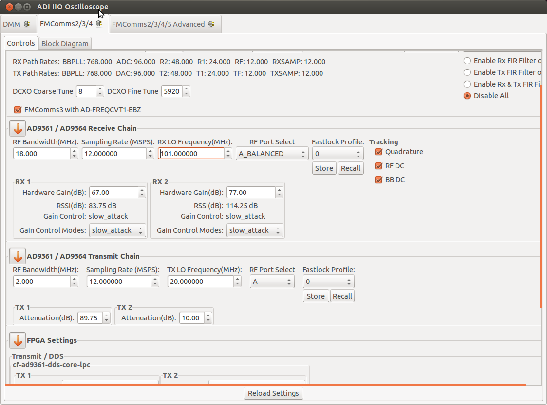
Two environmental variables allow the user to control the sign in the mixing equation as well as the window size (span) where the signal is centred around the SAW band pass filter center frequency.
ENV name |
default |
|---|---|
OSC_UPDN_FREQ_SPAN |
2MHz |
OSC_UPDN_FREQ_MIX_SIGN |
Positive |
Devicetree support
Function |
File |
|---|---|
FMCOMMS2/3 Device Tree |